DARPA asks industry for ways to blend electronic, photonic, and MEMS components on one silicon chip
Technologies developed in the E-PHI program should provide considerable performance improvements and size reductions over current state-of-the-art technologies, DARPA officials say. Of particular interest are low-noise electronic-photonic signal sources in the 20 GHz radio frequency band and in the 1,000-to-2,000-nanometer near-infrared optical band.
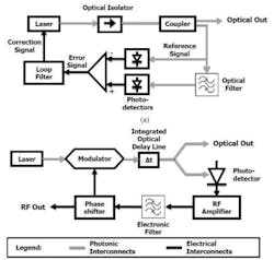
These kinds of technologies should provide markedly improved technologies for optical gyroscopes, direction finding, optical communications, and frequency reference synchronization for advanced high-bandwidth RF and mixed signal chip-integrated systems, DARPA officials say. The idea is to manufacture these technologies on existing silicon CMOS chip fabs.
Examples of potential approaches include micro-assembly, epitaxial layer bonding and printing, and direct epitaxial growth in silicon process flows. DARPA scientists anticipate that integrating photonics and electronics on a silicon substrate could help produce compact optical oscillators faster electronic feedback, enhanced coupling among photonic components, and better thermal and vibration tolerance than in technologies available today.
The E-PHI is divided into three parts: heterogeneous electronic-photonic integration process and device technologies; heterogeneously integrated electronic-photonic architectures; demonstration microsystems. Industry proposals that address all three areas are of particular interest, DARPA officials say.
The aim of the first part is to develop fabrication and device technologies to integrate different photonic and optoelectronic materials on a silicon CMOS-compatible substrate. Modular approaches are of particular interest, DARPA officials say.
The second part focuses on architectures and design approaches that take advantage of heterogeneously integrated materials and electronic and photonic devices. The third part centers on demonstrating microsystems based on technologies and approaches developed in the first two parts of the E-PHI program -- particularly continuous-wave and pulsed laser sources; RF optoelectronic signal sources; and other novel demonstration systems.
Companies interested should submit proposals no later than 3 June 2011. For questions or concerns, contact DARPA's Scott Rodgers by e-mail at [email protected], or by post at DARPA/MTO, ATTN: DARPA-BAA-11-45, 3701 North Fairfax Dr., Arlington, VA 22203-1714.
A proposer's day to brief industry and providing teaming opportunities will be 2 May 2011 in the Washington, D.C. area. Those interested in attending should register no later than 27 April 2011 -- one week away -- by e-mail at [email protected].
More information is online at https://www.fbo.gov/spg/ODA/DARPA/CMO/DARPA-BAA-11-45/listing.html.
