Nano-optics: robust, optical devices for demanding applications
By Hubert Kostal
Optical systems in defense and security applications must be able to deploy in harsh environments and meet demanding requirements for high performance and high reliability. In addition, demand continues for optical devices that are small, light, robust, and-to the extent possible-highly integrated.
Most often it is the optical portion of an electro-optic circuit or the electro-optic interface that represents the biggest design challenge for performance, efficiency, robustness, and cost. This is so because photons carry information in a different way than electrons do, and because they are not manipulated or guided the same way.
Conventional optics and optical engineering address these issues but have significant physical limitations, not the least of which involve materials; changing the material changes the function, and often can result in undesirable tradeoffs between material properties and optical functionality. Similarly, the mixture of individual optical component technologies that must be used often translates into minimal integration, so circuit designs are limited by component capabilities.
“Nano-optics” provides a new approach to meeting these requirements by creating a new class of optical devices with desirable optical effects through nanometer-scale structuring of various materials. Selecting appropriate structure designs and functions can yield a broad range of optical functions in a layer as thin as a few microns. Appropriate structure designs include one-, two-, or three-dimensional, regular or irregular structures. Appropriate materials include dielectrics, metals, and plastics. Possible optical functions include switching, spectral and polarization filtering, and phase modification.
Such nanostructure layers can be fabricated on a broad range of substrates so that manufacturers either can customize the optic to the application, or fabricate it on the surface of another optical component in an optical circuit. This approach can enable dramatic reductions in overall size and weight. Optical functions can be created using a broad range of materials, so manufacturers can select materials with performance under operating environments in mind.
Nanostructure-based optics
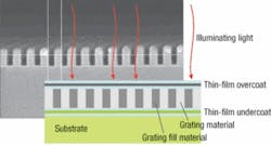
Nano-optics are optical thin-film structures that derive their physical properties by patterning materials on a subwavelength-scale roughly normal to the incident angle of the illuminating light. For ultraviolet, visible, and near-infrared wavelengths, the critical dimensions of these structures are on the nanometer scale. The structural attributes that determine the functional performance of a nano-optic device include:
- the nanopattern and its dimensions;
- the material used for the nanopatterned layer;
- the material used for the fill between the nanostructures;
- the formulation of the thin-film layers on either side of the nanostructure layer; and
- the substrate.
The critical dimensions of nano-optic structures for ultraviolet, visible, and near-infrared wavelength devices are on the order of tens to a few hundreds of nanometers, with a sub-ten-nanometer dimensional accuracy required in fabrication.
Physically, nano-optic devices derive their optical performance from the unique interactions of light with subwavelength-scale structures-including form birefringence and elimination of higher-order diffraction. At a macro level this is high optical performance in a grating layer often thinner than one micron. The optical function of nano-optic devices is the result of a convolution of material and structural properties, so the same optical function can be achieved using different material choices by making appropriate adjustments in the dimensions of the nanostructures.
Optical functionality that has been demonstrated based on nanostructures includes:
- polarization effects such as polarizers and polarization beamsplitters or combiners;
- phase retardation such as wave plates and retarders;
- spectral selection; and
- focal adjustment such as antireflection structures, diffusive layers, lenses, or mirrors.
In general, nano-optic devices can be designed to perform well in harsh environments by trading off material and structure to use the most robust possible material to achieve the desired function and to minimize the effect of thermal expansion or contraction.
Fabricating nano-optics
Nano-optic devices are fabricated using semiconductor-like deposition, lithography, etching, and coating processes. In general, a lithographic mask is prepared with the desired nanoscale features patterned on it. The original mask can be patterned using e-beam lithography, interference lithography, or by combining multiple partial mappings and exposures to create spatial variations or arrayed optics. Manufacturers can use this mask in a variety of methods to transfer the nanopattern to a target wafer; the specific topography of the mask depends on the method.
A fairly simple method is nanopattern transfer lithography, which is closely related to nanoimprint or nanoembossing. Nanopattern transfer uses physical contact to transfer a pattern to a resist layer. This approach allows for high fidelity in pattern replication, and avoids interactions between an energy beam and the polymer layer that can reduce the accuracy of the pattern transfer. The nanopattern transfer manufacturing process consists several steps.
First, one or more target wafers are prepared by selecting a substrate material, depositing appropriate thin-film boundary layers, and depositing an appropriate thickness of a target material. This target material is the layer into which the nanostructure is to be inscribed; usually it is a dielectric or a metal layer.
For each wafer, a thin, pliable, polymer resist layer is spun on top of the target layer, then a physical “mold” shaped with the complement of the desired pattern is brought into contact with the resist. The polymer resist layer is then set using ultraviolet or thermal curing, and the mold removed. This leaves a relief of the desired pattern in the now fixed polymer resist layer.
The fixed polymer resist layer then acts as an etching guide to transfer the pattern to the underlying target layer. After etching has been completed, various deposition processes fill the etched areas with a second material and add a thin-film boundary or surface layer. It is important to eliminate any voids and microchannels in this process.
Finally the wafer can be diced to size for application, or can be used as the base substrate for another deposition and etching cycle to create multilayer, multifunction, nano-optic devices.
Nano-optic integration
This semiconductor-like wafer-scale fabrication process facilitates the application and integration of nano-optic devices into general electro-optic circuits. Three types of integration can take advantage of nano-optics.
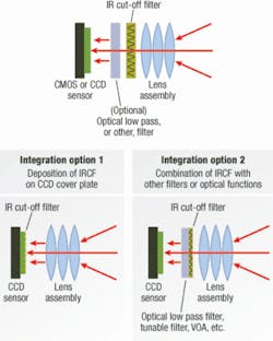
First of these is integration by assembly. For certain applications, the nano-optic device will be fabricated on a glass or other substrate whose primary role is to act as a holder for the nano-optic structure. By appropriate material and optical design, this structure can be designed to allow reduced spacing between the nano-optic and adjacent devices to be reflective or to have a broad tolerance for angle of incidence to reduce or eliminate the effect of general assembly misalignment. One or more of these effects can permit the optical circuit to be more robust or smaller in size.
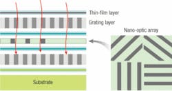
Second is monolithic integration. Nano-optic layers can be interspersed with thin-film layers and configured in arrays of optical functions.
Third is hybrid integration. In many cases, the nano-optic layer can be applied to other optical materials or to pre-existing surfaces in an optical design. This eliminates the need for the substrate for the nano-optic device, allowing reduction in size of the optical circuit. Combining nano-optic layers with appropriate electronically reconfigurable layers, such as liquid crystal, lithium niobate, or MEMS structures can allow the design of highly compact electronically tunable optics, such as variable optical attenuators, optical switches, and tunable filters.
Applications of nano-optics
Nano-optic devices can be applied to a broad range of optical circuits, such as digital imaging systems, projection display systems, and optical sensors.
For digital imaging systems, nano-optic filters can provide increased performance and robustness. Applicable nano-optic devices include bandpass filters, polarizers, waveplates, tunable spectral filters, and optical low-pass filters.
For projection display systems nano-optic devices can improve picture clarity and contrast in devices such as polarizers, polarization beam splitters, band-pass filters, and waveplates.
In optical sensors, sample response to single-wavelength or broadband light sources can be used to identify potential threats or contaminants. Applicable nano-optic devices include polarization beamsplitters, polarizers, waveplates, and spectral filters. Nano-optic tunable filters can be considered for hyperspectral sensing.
For all of these applications, monolithic or hybrid integration of nano-optic devices can reduce the size and weight of optical circuits.
In general, nano-optics provides a relatively new approach to creating optical devices with many more degrees of freedom in material selection, performance, and integration than available using classical optics. The flexibility that this affords the electro-optic circuit designer often permits improved performance, improved reliability, and reduced size and weight through optical integration. Many of the applications for this technology are just now being considered, so this remains a fertile area for exploration and discovery.
Hubert Kostal is vice president of marketing and sales at NanoOpto Corp. in Somerset, N.J. For more information contact the company online at www.nanoopto.com.


