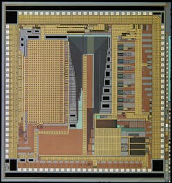
ARLINGTON, Va. - U.S. military researchers are asking integrated circuit (IC) experts at the University of Southern California (USC) to help revolutionize high-end custom IC design for military and aerospace applications.
Officials of the U.S. Defense Advanced Research Projects Agency (DARPA) in Arlington, Va., announced an $11.8 million sole-source contract to the USC Information Sciences Institute in Los Angeles for the Circuit Realization at Faster Timescales (CRAFT) - FinFET Foundry/Design Aggregation Services military chips program.
The U.S. military is developing systems that require high computational performance in a power-constrained environment; yet, these technologies cannot be manufactured fast enough. Systems designers today must choose between high performance and low power consumption. Often systems designers must choose between a high-performing, custom IC that requires years to design and fabricate, or settle for a lower-performing processor programmed in months.
The DARPA CRAFT program seeks to demonstrate a custom IC design flow and methodology in a leading- edge commercial 16- or 14-nanometer fab, port these designs to new foundry process flows, and increase design reuse by providing a repository for secure storage and distribution of design elements.
The CRAFT has three technical goals: reducing custom IC design and fab cycle time by 10X with new software tools; enabling a 50 percent reuse of critical military IC modules with an intellectual property (IP) repository system; and enabling flexible chip fabrication by porting a technology node from one foundry to another, or migrating from one design node to another design node at the same foundry. To meet these goals, DARPA needs to build custom ICs using the FinFET leading-edge CMOS process node because of this technology's density, performance, and power advantages. To access this technology, the CRAFT program needs FinFET foundry access, and this is where USC Information Sciences Institute comes in.
USC will provide a design aggregation service for CRAFT contractors; collect individual designs, produce an aggregation of these designs to create the floorplan for the full mask set, and insert test structures to provide vital early assessment of the designs; and train military and university designers on using the technology.


