By John Rhea
Once the digital electronics industry featured a plethora of board manufacturers that specialized in single-board digital signal processors. Today, these same board manufacturers are re-inventing themselves into subsystem designers and systems integrators, which confronts them with a broad range of cooling, power, and software issues.

Mixing and matching analog and digital functions with multi-chip modules continues to challenge military and aerospace electronics designers as commercial applications drive new approaches for defense, aviation, and space hybrid devices
Mixing and matching analog and digital devices in the same systems — and sometimes even on the same integrated circuit — has been a challenge for military and aerospace designers for the past 30 years since the dawning of the age of microprocessors.
The heart of the problem involves the front-end analog sensors, notably radar and infrared. These sensors struggle to keep up with the exponentially increasing speeds of the back-end digital processors. It has thus become imperative to digitize the analog representations of the "real world" as far up front in the system as possible in order to feed data to the voracious processors.
That is essentially what the sensors of the human body do, and that is why the optic nerve has the shortest possible signal path to interface with the brain. The world is, after all, analog, and the optic nerve is a high-throughput analog-to-digital (A-D) converter that moves most of the information from the visible portion of the electromagnetic spectrum (the eyes) to the three-pound central processor (the human brain). In this context, the brain is the ultimate mixed-signal processor.
In the case of military systems, the hardware for the A-D job has evolved from the Microwave and Millimeter Wave Integrated Circuit (MIMIC) program of the Defense Advanced Research Agency (DARPA) in Arlington, Va., in the 1980s. Following on to the MIMIC program was a DARPA effort in late 1995 called Microwave and Analog Front End Technology (MAFET).
The ultimate hybrid packaging for avionics applications, therefore, might include multichip modules (MCMs), digital and microwave integrated circuits, transformers, flowing cooling fluids, optical and copper cables and connectors, as well as embedded software.
A typical example is a Global Positioning System (GPS) receiver with a gallium arsenide (GaAs) analog front end, a complementary metal oxide semiconductor (CMOS) signal processor, and a crystal oscillator.
John Hartman, president of Worldwide Business Associates, a consulting firm based in Eaton Center, N.H., focuses on MCMs as the solution to this problem. "In my opinion the MCM is probably one of the best techniques for COTS [commercial-off-the-shelf] applications of integrated circuits," he says.
The reason, Hartman explains, revolves around rapid technology insertion. MCMs, he says, enable users to select commercial-grade chips to achieve desired levels of functionality and then simply upgrade those chips as new technology becomes available, thereby circumventing the obsolescence problem. Hartman was formerly a military marketing expert at Analog Devices Inc. in Norwood, Mass.
"You can combine the functions on an appropriate substrate in hermetic packages and qualify the whole unit to the customer requirement," notably MIL-STD 883, he adds. "You can take advantage of all the technology available in a single package."
There are tradeoffs here. For consumer products such as cellular telephones and camcorders, with their requirements for high performance and their potentially high volumes, it is possible to apply "system-on-a-chip" approaches in which in which the A-D and digital signal processing functions combine on one piece of silicon.
That approach is sufficient for the high-volume commercial applications in which the non-recurring engineering (NRE) costs amortize over a long production run and where there is ample opportunity to proceed down the experience curve. Yet the relatively low-volume military applications, with their higher performance requirements, would require greater use of custom chips at inherently higher costs throughout the life cycle. Also, the greater chip complexities would initially hold down yields, and there would not be sufficient volume to push yields up to economical levels, hence the growing popularity of MCMs for military and aerospace users.
DARPA-sponsored researchers have found that conventional packaging techniques are struggling to keep up with rapidly increasing system performance requirements. Originally that involved only supercomputers, but today even mid-range systems have interconnection limitations. Smaller systems, such as today's booming generation of portable communications and computing devices, demonstrate that problem dramatically.
Furthermore, according to DARPA, the cost of packaging (traditionally about 10 percent of chip cost), assembly, and test is now approaching the cost of the die. The single-chip approach also poses several penalties. In power, for example, chip-to-chip interconnects account for 15 to 40 percent of system power consumption. Where system space is concerned, silicon accounts for only 5 to 25 percent of the board area. Reliability is also a concern because module-to-board solder connections account for 80 to 90 percent of board failures.
MCMs address these shortcomings by eliminating the first level of packaging for many components, the DARPA research discloses. Some expected gains are an increase in gates per module of 10 to 100 times, increase of input/output per chip of 10 to 100 times, reduction in board area of 3 to 10 times, improvement in system reliability of 10 to 100 times, and reduction in system power consumption of 10 to 30 percent. Another anticipated benefit of MCMs is a reduction in the electromagnetic interference from printed circuit boards.
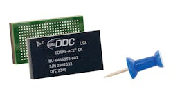
This mixing and matching approach is exemplified by the work of Data Device Corp. (DDC) of Bohemia, N.Y., a leader in the 1553 databus field. Mike Glass, product manager for the firm's Fibre Channel line, explains that DDC engineers are using MCMs in their current products that combine custom-designed applications-specific integrated circuits (ASICs) that meet military temperature specifications, as well as in COTS memory chips.
DDC engineers design their transceivers with the BICMOS process, then combine these devices with the static random access memories (SRAMs) — typically 64 K by 16 bought from outside vendors as die — in a co-fired flat pack ceramic package that is 1 inch square. These are chip and wire hybrids, Glass explains, which offer the MCM advantage of miniaturization.
DDC device designers use the technique throughout military platforms, such as the F-16, F/A-18, and F-22 fighter aircraft, as well as the M1A2 main battle tank. They are even finding an application for this technique in the International Space Station, which also uses the MIL-STD 1553 databus.
Looking beyond today's 1-megabit-per-second 1553 applications, Glass says he hopes to extend the technology to the projected multi-gigabit Fibre Channel databuses of the future. A candidate packaging technique for the MCMs is ball grid arrays, and he envisions devices capable of combining electrical functions with the optical functions necessary for those greater throughputs.
Sounding a note of caution regarding MCMs, however, is Duncan Young, director of marketing at DY 4 Systems, a VME printed circuit board designer in Kanata, Ontario. Young says his company used to use MCMs five years ago but does not do so today. The reason, he says, is the necessity to achieve relatively high volumes. He agrees that MCMs are best for sophisticated parts that require high packaging densities. Yet in his experience these tend to be in applications in which, as he puts it, "money is almost no object."
This means that lifetime buys are required by some weapons systems to combat the obsolescence problem. Given the long lifetimes of those systems and the rapid product cycles of the components, Young says, there is the potential problem that the parts in the MCM will become obsolete by the time the program achieves initial operational capability.
"It's all a tradeoff between time to market, cost, and packing density," Young says. He places a high premium on time to market, and therefore says he is reluctant to invest in ASICs. Instead, DY 4 prefers what he calls bigger and better field programmable gate arrays, or FPGAs, for special functions.
Like all vendors in this market, DY 4 is in the intellectual property business, Young points out. Therefore, systems designers must restrict the complexity necessary for advanced packaging to functionalities that they cannot achieve any other way.
Other applicationsSteve Summer, president of Modular Devices Inc. of Shirley, N.Y., sees another application of advanced hybrid packaging techniques that is spinning out of today's military and aerospace market: down-hole oil well sensors.Although the company is primarily a supplier to military and aerospace applications, Summer says his company is moving into the energy field, which is growing rapidly due to current world conditions. Modular Devices makes a line of power supplies in integrated packages capable of meeting the high-temperature requirements of oil wells, typically around 200 degrees Celsius, while staying within the size limitation of the drills, typically around one and a half inches.
Like DDC, Micropac Industries Inc. of Garland, Texas, has an application of MCMs on ceramic substrates aboard the International Space Station, but of a different sort. The company has used the hybrid packages on a variety of missile programs, for example, to achieve stage separation for the Titan launch vehicle, says Norm Dang, engineering manager.
The company's package serves as an environmental control application aboard the Space Station. This is a thermostat that receives inputs from the resistive temperature device, detects the signal, and then turns the station's heaters on and off in the astronaut quarters and cargo bay.
These are typically eight-pin dual-in-line packages measuring an inch or two on a side, according to Dang. Company engineers combine active and passive devices in the same package. The packages are qualified to the temperature specifications of the station, which are actually less demanding than those for down-hole oil well applications.
National Hybrid Inc., based in Ronkonkoma, N.Y., has launched an MCM program at its Pace Technology Inc. subsidiary in Largo, Fla. Kevin Mussmacher, director of business development, says the goal is to integrate analog circuitry with high-density digital devices.
National Hybrid experts do this with a ceramic module, using chip and wire assembly of specific die. Mussmacher claims the approach cuts costs and development cycles. The MCMs have a 0.002-inch metallization line width with 0.002-inch spacing between metallization signal traces.
Packages with as many as 284 pins and ASICs with more than 400 bond pads are in production, he adds. The ASICs are custom, and the digital processors, SRAMs and other memories, and 1553 interfaces are combined with them. The hermetically-sealed packages eliminate glass-to-metal feed throughs, and the packages are screened to the U.S. government performance standard MIL-PRF-38534.
California Eastern Laboratories (CEL) in Santa Clara, Calif., produces commercial-grade hybrid packages for telecommunications applications and has achieved its highest level of integration for a GPS receiver. It uses a 3-volt power supply, 16 MHz crystal reference, and is contained in a 36-pin package — including a 23 GHz bipolar transistor.
CEL engineers also are working on MCMs for handset power amplifier applications as a custom project, says spokesman Mark Navarre. Yet Navarre says he hopes to develop generic modules for the general market. CEL also offers three gallium arsenide field effect transistor devices from Nippon Electric Corp. for mobile satellite radio antenna applications.
Experts at C-MAC Microtechnology of Durham, N.C., have developed a family of MCMs using multilayer thick film materials, originally for military aircraft as a gateway to interface such subsystems as pilot controls, control surfaces, avionics, computers, and weapon systems on a common databus for fly-by-wire pilot control.
Janet Kingston, a promotional marketing executive based in the company's Purcelville, Va., office, reports that although MCMs have no clearly agreed definition, in general they are considered to be high-density packaging of bare semiconductor devices. The company began using ceramic thick film substrates with wire-bonded dies in hermetic cavity packages.
The technology is migrating to other applications, and substrates now include epoxy laminates and thin films. Epoxy and silicone are now being used as a means of protection, and wirebonding is beginning to be replaced by flip-chip assembly.
A key advantage of this approach is the elimination of non value-added packaging of bare die, according to C-MAC. The packaging and interconnection of a module can add a factor of 100 to the size of the functional areas of the active and passive components, Kingston notes.
TRW using InP in new power amplifiersREDONDO BEACH, Calif. — TRW's new semiconductor company, Velocium, and Hitachi Ltd. of Tokyo are employing indium phosphide (InP) semiconductors in a new line of power amplifier modules for third-generation wireless handsets and other wireless applications. Sampling of the devices is scheduled for early next year.Experts will build the chips at TRW's Velocium facility in Manhattan Beach, Calif., and Hitachi will manufacture the modules. InP technology was chosen because of its inherent power efficiencies that are more than 50 percent greater than conventional devices, according to TRW. This is intended to provide the signal quality required for wideband CDMA applications.
Under the agreement, signed in May, both companies will participate in the design and development of the modules, contributing existing proprietary designs and developing new designs. Volume production is planned for the second half of next year. — J.R.
DARPA integrating silicon, 3-5 compounds in moduleARLINGTON, Va. — A research program in progress at the Defense Advanced Research Projects Agency (DARPA) in Arlington, Va., aims at achieving the functional density of complementary metal oxide semiconductor (CMOS) devices with the speed of such compounds as gallium arsenide and indium phosphide — plus integrating photonic devices into the packages.The program, known as heterogeneous integration of materials with silicon, combines batch fabrication with monolithically assembled integration. One of the ground rules is that the fabrication process has to be compatible with silicon CMOS.
The goal is to provide multi-function radio frequency circuits via monolithic assembly, according to the DARPA program manager, Daniel Radack, in the agency's Microsystems Technology office.
As is common with DARPA programs, this is predominantly a university effort, with the University of Wisconsin, California Institute of Technology, North Carolina State University, Princeton University, Columbia University, and Massachusetts Institute of Technology working on the batch fabrication, and the University of California at Berkeley and Massachusetts Institute of Technology working on the monolithic integration. However, such corporations as Motorola, Boeing, and Northrop Grumman are also involved.
The gallium arsenide layer is actually grown on top of a sandwich of germanium and silicon germanium in an attempt to reduce defect density and increase carrier lifetimes. — J.R.
Who's who in hybrids and hybrid packagingAnalogic Corp.Peabody, Mass.978-977-3000http://www.analogic.com/Apex Microtechnology Corp.Tucson, Ariz.520-690-8600http://www.apexmicrotech.com/C-MAC MicroTechnologyDurham, N.C.919-941-0430http://www.cmac.com/mt/index.htmlCalifornia Eastern Laboratories (CEL)Santa Clara, Calif.408-988-3500http://www.cel.com/Data Device Corp. (DDC)Bohemia, N.Y.631-567-5700http://www.ddc-web.com/Film Microelectronics Inc. (FMI)North Andover, Mass.978-975-3385http://www.filmmicroelectronics.com/Micropac Industries Inc.Garland, Texas972-272-3571http://www.micropac.com/Modular Devices Inc.Shirley, N.Y.631-345-3100http://www.mdipower.com/National HybridRonkonkoma, N.Y.631-981-2400http://www.nationalhybrid.com/Omnirel LLCLeominster, Mass.978-534-5776http://www.omnirel.comQ-Tech Corp.Culver City, Calif.310-836-7900http://www.q-tech.com/Teledyne Electronic TechnologiesLos Angeles310-822-8229http://www.tet.com/Velocium, a TRW CompanyManhattan Beach, Calif.310-814-5749http://www.velocium.com/