by J.R. Wilson
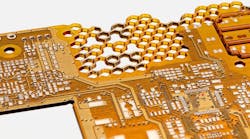
PALO ALTO, Calif. — Industry and university scientists are taking aim at the next generation of integrated circuit packaging, with a goal of building chips that are smaller than ever before.
Researchers at Hewlett-Packard in Palo Alto, Calif., and at the University of California at Los Angeles (UCLA) won a U.S. patent for technology they say could lead to the production of molecular-scale complex logic chips.
These devices eventually could replace silicon-based integrated circuits, which experts say may reach their physical and economic limits in about 10 years.
The patent is based on previous patents and work performed under a grant from the Defense Advanced Research Projects Agency (DARPA) in Arlington, Va., which anticipates significant military applications for such nano-chips.
Rather than the complex pattern of wires that now define a computer circuit, the HP/UCLA approach would replace that high-cost manufacturing process with a simple grid of wires, each only a few atoms wide, connected by single-molecule electronic switches. This follows a previous HP laboratory demonstration in which some rare earth metals, when reacting chemically to a silicon substrate, naturally form nanoscopic parallel wires.
In a related experiment, HP/UCLA scientists sandwiched current computer chip-size wires around a one-molecule thick layer of electrically switchable molecules called rotaxanes. Downloading signals to molecules trapped between the crosswires electronically created simple logic gates.
"That work demonstrated for the first time that molecules could be used as electronic devices to perform computer logic," says UCLA chemistry professor James Heath, director of the California Nanosystems Institute and one of the patent-holders.
"All of this work demonstrates that, in the future, programming could replace today's complex, high-precision method of fabricating computer chips," adds another of the patent team, HP Labs senior scientist and computer architect Philip Kuekes. "Once a basic grid has been assembled, programming could be used to implement a very complex logic design by electronically setting the appropriate configuration switches in the molecular-scale structure."
Previous efforts to create complex chips in this fashion failed because the electrical signals on a single large grid interfered with each other, explains HP Fellow R. Stanely Williams, director of quantum science research for HP Labs, and the third member of the patent team.
"It would be like removing all the traffic signals from Manhattan and demanding a minimum speed of 30 miles per hour — the result would be total gridlock," Williams says. "Signal lights, or cut wires, regulate the flow of traffic and make it possible to carry passengers, or information, between any two points on the grid.
Williams says the Team's solution is to cut the wires into smaller lengths by turning some of the "intersections" into insulators, created by giving the cutter and target wires different voltages. "Essentially, you subdivide the city into smaller neighborhoods, with smaller local streets within each neighborhood and larger streets connecting the neighborhoods."
HP officials predict the first niche applications for nano-chip technology — used in combination with advanced silicon-based circuitry — could be available in dense memory within five years.