By Tom Adams
BERLIN - One potential benefit of shrinking the sizes of microelectronics components is the potential to scatter a large number of sensors arranged as a distributed array over an area for surveillance. In theory, an intruder triggers one or more simply because so many sensors are in the area.
The reality, however, is the difficulty that designers have in assembling a useful distributed sensor network from off-the-shelf parts. Some basic and rather severe requirements are preventing immediate deployment: the sensors must be very small, very robust, and very inexpensive.
Miniaturization techniques for integrated sensor packages began some years ago at Berlin’s Fraunhofer Institute for Reliability and Microintegration (IZM), and has now reached a promising stage.

The work at Fraunhofer IZM focuses on advances in semiconductor packaging, but not on developing specific applications. “We are concerned with the three-dimensional integration of electronic packages, which means shrinking the package dimension in the vertical dimension as well as the horizontal dimensions,” says Andreas Ostmann, a physicist at Fraunhofer IZM.
The package containing the sensing, communications, and power elements must become smaller yet remain fully integrated. The Fraunhofer team is taking advantage of existing packaging technologies, developing new packaging techniques, and will incorporate new packaging methods as they become available. Their concentrated approach to packaging, with emphasis on size, costs, and robustness, may be a workable model for other electronics systems as well.
The cube-shaped sensor package under development is called the eGrain to suggest the truly miniature dimensions that the Fraunhofer team hopes to achieve. Currently, the sensor device consists of a tiny battery, a miniature microcontroller board with an antenna, and a sensor. The integrated sensors tested to date respond to light intensity, field strength, or thermal changes.
Steps in miniaturization
The prototype cubic eGrain measures about one inch on a side. At these dimensions, engineers fabricate the cube with standard surface-mount microelectronic packaging processes, and could manufacture it with existing packaging equipment.
The next stage in miniaturization will shrink the sensor package to about 0.8 inch per side. At this size, the package will use flip-chip fabrication instead of more conventional components to take advantage of the high density of I/Os that a flip chip can deliver. The package will still be manufacturable via existing surface-mount methods.
Late in 2004 the eGrain will shrink again to 1 centimeter per side, or about the size of a raisin. At this level of miniaturization, fabrication of the cube will depart from conventional surface-mount methodology and will converge with alternate packaging methods also being developed at Fraunhofer IZM.
“Those are the near-term goals, but we think we can go beyond this and reduce the entire package down to a 5-millimeter cube, Ostmann’s colleague Stepan Guttowski observes. These dimensions will bring the eGrain down close to the size of a grain of wheat, the item after which it has been named.
Fraunhofer is intent on making the units so inexpensive that the cost of distributing large numbers will not be burdensome. Steve Martell, chairman of one of the IPC’s component groups, points out that the early production is unlikely to achieve low cost. “There are always process problems to be worked out, and the size of the package means that the parameters involved will be very small. True low-cost volume production should be possible after these problems are solved.” But Martell also observes that IPC standards are still evolving for packages having such small dimensions.
Deployment And Communication
Distributing the sensor units may actually amount to dropping them from a helicopter to saturate a specified area. Somewhere among the sensor array will be one large control and relay system. Each individual eGrain will have its own energy source, even when the size drops to the 5-millimeter level. The eventual energy source may be a tiny lithium ion battery or a solar cell, but it will obviously be necessary for the units to operate on minuscule amounts of energy if they are to have respectable service lifetimes.
Developments in solar cell technology may help to solve this problem. “Work is under way now on organic photo-voltaics,” notes Katherine Derbyshire, founder and president of Thin Film Manufacturing, a business and technology analysis firm in Stoneham, Mass. “This would make it possible to wrap the entire eGrain in what amounts to a solar cell, so you wouldn’t have to worry about it landing right side up. Not all of the surface would be exposed to light, of course, so the energy requirements would have to be met by roughly half of the surface area.”
Coiled within the e-grain will be an antenna. The length of the coil determines the optimum wavelength for communication transmission. Ideally, the length of the antenna should be about one-quarter the wavelength at the frequency selected. For example, the wavelength of a 3-GHz signal is about one-tenth meter, and the total length of the coiled antenna would have to be about approximately 25 millimeters, or 1 inch.
Coiled antennas are not an efficient solution for future miniaturization of the device because of the shielding effect of the battery and the electronic layers. Hence, for further miniaturization alternative antenna shapes like a folded patch or a slotted waveguide antenna will be used.
Very high frequencies - 10 to 20 GHz - would reduce the size of the antenna, but at these frequencies radio waves begin to behave more like light waves, and cannot easily penetrate objects such as bushes. The final frequency will be a compromise between antenna size and useful frequencies. An external antenna - a wire trailing from the cube - is a possible alternate route for antenna design.
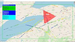
Most of the sensors in an array will communicate not with the central control and relay, but with each other. In this way the energy expended by each unit can be kept to a minimum. Each unit will be required to transmit over a distance of a few meters to its nearest neighbor rather than 100 meters or so to the control center.
One of the more difficult parts of future development will be writing the software to control an array of hundreds or thousands of eGrains in the field. The software to control the whole array is of a type known as data fusion. Programming for data fusion is very complex but achievable.
It will also be necessary to establish the precise position of each of the hundreds or thousands of units in order to ascertain the origin of a given signal. At the moment, it isn’t feasible to place a GPS unit in each eGrain, but there may be a more efficient way of determining location.
A sensor signal diminishes in strength according to the square of the distance between the sensor and the receiver. Reading the signal strength at two sensors should give the location of a third sensor. Software triangulation using the signals from the sensors adjacent to one another is then used to define the locations of all sensors in the array.
Achieving manufacturability
As the dimensions of the eGrain shrink, it will demand assembly techniques that are not yet the standard in board assembly, but which have been evolving in other semiconductor sectors. Stacking of microprocessors and memory modules to reduce size and increase performance speed is currently in production as one example of successful 3-D integration technology.
The Fraunhofer Institute is involved in several areas of 3-D integration of semiconductor packages, and one of the areas under development works at shrinking the vertical dimension of packages. “There is some urgency in this work because mounting components of ordinary thickness on a PC board results in a package that is too thick for next-generation cell phones, the eGrain, and other advanced applications,” Ostmann explains.
One promising area of development is called CIP, for Chip in Polymer. The basic idea is fairly simple: experts thin down a silicon chip to 50 microns and adhesively bond it to a PC board. Then they screen-print resistors onto the board as well. Then the experts cover the chip and resistors with a very thin layer of dielectric epoxy, and drill holes into the epoxy with a laser aimed from above to create vias for interconnections. They then mount additional components onto the epoxy layer.
Parts of this technology already exist. PC boards are available that have embedded resistors, and the thinning of silicon chips to 50 microns has become standard in several applications, and 10 microns has been achieved. Extreme thinning can take advantage of the flexibility of a very thin silicon wafer.
“Backside processing of completed device wafers includes a variety of steps,” explains Dr. Sharon Farrens of Austria’s EV Group. “These steps include thinning of the device layer, backside ion etching, lithography, and even metal deposition. To adequately protect the finished front side of the device wafer during these aggressive fabrication steps, the device wafer is generally attached to a support or carrier wafer such as silicon, sapphire or quartz. A protective coating is used to inhibit direct contact of the front surface with the carrier wafers. Then the device wafer is attached using any number of adhesives.
“The adhesive choices include waxes and liquid polymers, dry films that are thermally or UV released, and solvent released products. Many of these methods were developed for lapping of compound semiconductor substrates.”
Also under investigation at Fraunhofer are new methods of fabricating the bumps that connect a flip chip to a board. Engineers can take the best advantage of shrinking silicon design rules if they can also miniaturize the size of interconnects, especially for flip chips. Fraunhofer has already tested flip chips where the solder bumps are only 8 microns wide and spaced 7 microns apart, numbers that compare favorably to today’s 75-micron width and 75-micron spacing for flip-chip bumps. Perhaps even more impressive, these bumps are only 1.5 microns thick - another big step toward vertical integration.
Ostmann and Guttowski anticipate that assembly and packaging costs will be about equal to the silicon costs. The evolution of new assembly techniques, along with high-volume production, can make the eGrain inexpensive as well.