Purdue researchers develop material for better optics, communications
By John McHale
WEST LAFAYETTE, Ind. - Engineers at Purdue University say they are the first researchers to create a material that has a “negative index of refraction” in the wavelength of light used for telecommunications, a step that could lead to better communications and imaging technologies.
The research, funded by the U.S. Army Research Office and the National Science Foundation, is affiliated with Purdue’s Birck Nanotechnology Center-the university’s hub for interdisciplinary research.
“This work represents a milestone because it demonstrates that it is possible to have a negative refractive index in the optical range, which increases the likelihood of harnessing this phenomenon for optics and communications,” says Vladimir Shalaev, the Robert and Anne Burnett Professor of Electrical and Computer Engineering at Purdue in West Lafayette, Ind.
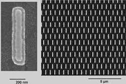
The material consists of tiny parallel “nanorods” of gold that conduct clouds of electrons called “plasmons” with a frequency of light referred to as the near-infrared, Purdue researchers say. The wavelength size of this near-infrared light is 1.5 microns, or millionths of a meter, the same wavelength used for fiber-optic communications. “This is the most important wavelength for communications,” Shalaev says.
A major obstacle hindering development of optoelectronic devices is the wavelengths of light, which are too large to fit into the tiny features necessary for miniature circuits and components. Plasmonic nanomaterials, however, could make it possible to squeeze light waves into much smaller spaces, Shalaev said.
Research groups have fabricated “metamaterials” made of tiny metal rings and rods, which have a negative index of refraction. No metamaterials have yet been created that have negative refraction indices for visible light.
Now, however, the Purdue researchers have created a metamaterial with a negative refractive index in the near-infrared portion of the spectrum. This is just beyond the range of visible light, demonstrating the feasibility of applying the concept to communications and computers.
The nanorods are an example of materials that are able to reverse a phenomenon called refraction, which occurs as electromagnetic waves, including light, bend when passing from one material into another and is caused by a change in the speed of light as it passes from one medium into another.
Scientists measure this bending of radiation by its “index of refraction.”
Refraction causes the bent-stick-in-water effect, which occurs when a stick placed in a glass of water appears bent when viewed from the outside. Each material has its own refraction index, which describes how much light will bend in that particular material and defines how much the speed of light slows down while passing through a material. All natural materials, such as glass, air, and water, have positive refractive indices.
In 2000, researcher John Pendry at the Imperial College London theorized that slabs of such material might be used to create a “superlens” that would drastically improve the quality of medical diagnostic imaging and other technologies, Purdue researchers say.
Such lenses theoretically could compensate for the loss of a portion of the light transmitting an image as it passes through a lens. Harnessing materials that have a negative index of refraction could make it possible to take optical images of objects that are smaller than the wavelength of visible light-including molecules such as DNA-for research and medical imaging.
Also possible could be “photo-nanolithography,” which would make it possible to etch smaller electronic devices and circuits, resulting in more powerful computers, as well as new types of antennas, computer components and consumer electronics such as cell phones that use light instead of electricity for carrying signals and processing information, resulting in faster communications.
“The challenge was to fabricate a structure that would have not only an electrical response, but also a magnetic response in the near-infrared range,” Shalaev says.
The gold nanorods conduct clouds of electrons, all moving in unison as if they were one object instead of millions of individual electrons. These groups of electrons are known collectively as plasmons. Light from a laser or other source shined onto the nanorods, inducing an “electro-optical current” in the tiny circuit. Each of the rods is about as wide as 100 nanometers, or 100 billionths of a meter, and 700 nanometers long.
“Although many researchers are skeptical about developing materials with a negative index of refraction in optical wavelengths and then using them in practical technologies, I think the challenges are mainly engineering problems that could eventually be overcome,” Shalaev says. “There is no fundamental law of physics that would prevent this from happening.”
Findings are detailed in a paper appearing Dec. 15 in Optics Letters of the Optical Society of America. The paper is by Shalaev, his graduate research assistants Wenshan Cai and Uday K. Chettiar, doctoral student Hsiao-Kuan Yuan, senior research scientists Andrey K. Sarychev and Vladimir P. Drachev, and principal research scientist Alexander V. Kildishev.


