By Keith Gurnett and Tom Adams
One of the least flexible rules in electronic design is the need to keep silicon devices, and compound semiconductor devices separate, not only in processing but also in assembly. If a system requires, for example, the technologies of gallium arsenide (GaAs) and silicon to achieve the required functionality, then you will need two chips, probably arranged in a multichip module.
Two new developments are now threatening to make this rule partly or entirely obsolete. One of these developments inserts a tiny compound semiconductor “chiplet” into a prepared area on the face of a silicon chip. The second development goes further by permitting processing of silicon and gallium nitride (the only feasible material to date) on the same wafer.
One area that can benefit from what are essentially multisubstrate chips is the development of X-band radar. This form of radar is for defense and attack applications involving incoming and outgoing missiles. The short wavelength enables very high-resolution imaging for target identification and discrimination.
Experts anticipate that X-band radar will use phased arrays, in which a group of antennas is arranged so that users essentially can steer the beam from a stationary transceiver. The relative phases (direction and relationship) create a radiation pattern that can achieve a 3-D scan. These three dimensions can be controlled electronically or mechanically to highlight a particular aspect of the scanned picture. Used for surface detection at sea or for missile control and targeting, X-band radar should be able to detect and track small objects over a range of 3,000 miles.
Integrating chiplets based on III-V materials with CMOS chips is the goal of the COSMOS (Compound Semiconductor Materials On Silicon) program recently launched by the U.S. Defense Advanced Research Projects Agency (DARPA) in Arlington, Va. Basically, DARPA is looking for companies that can develop successful assembly techniques. One open question is the method of interconnecting the III-V chip to the larger silicon chip. One approach uses an additional layer of metallization to form the interconnects, but other early efforts have used wire bonding, which is fundamentally easier and which requires less precision in the etched depth of the cavity into which the III-V chip is placed.
A second-and probably even more significant-problem is the method of attaching the III-V chiplet to the silicon. Normal thermal cycling will cause inevitable differential expansion and contraction between the III-V material and the silicon, and there will be a strong tendency for the III-V chiplet to pop out of its cavity. Presumably this problem is at the center of DARPA’s attention. The word on the street is that DARPA will be most interested in InP chiplets, presumably for photovoltaic requirements.
The chiplet approach
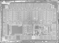
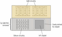
The basis of this approach is a silicon die with a reasonably large area. In the design of the die, one unpatterned area is set aside for the chiplet. When silicon processing has been completed, the chiplet area is etched or micromachined to a given depth, and the compound semiconductor chiplet is placed in this shallow cavity. The chiplet is then connected with the larger silicon chip, either by wire-bonding (the easiest method), or by laying down one additional layer of redistributed metallization. The chiplet is typically considerably smaller in area than the silicon die.
Some of the most advanced development of the chiplet concept is being carried out by Prof. Vincent Fusco in the Institute of Electronics, Communications and Information Technology (ECIT) of Queen’s University in Belfast, Northern Ireland.
One of the obvious challenges in the insertion of a chiplet into a larger die of a different species is management of the differences in coefficient of thermal expansion between the two materials. In his earlier work, Fusco simply epoxied the smaller III-V die into a cavity in the silicon die, but more recently he has developed a more suitable method.
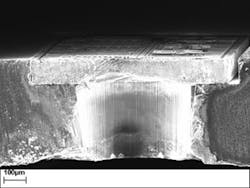
“We take a silicon substrate and we dry-etch it on the front in order to form a die-size cavity,” he explains. “Then we etch it from the back to form a via, and then we through-hole plate the via. We temporarily mount the III-V die using tape, and then we plate from the back metal contact of the die-we use the back metal contact as the seed layer, then we plate up.”
The end result is a copper plug behind the die that holds the chiplet in place and removes heat from the chiplet.
Fusco works with a 4-inch-diameter silicon wafer. The GaAs die are made by commercial foundries to his design. The silicon wafer is typically 400 to 600 microns thick, while the GaAs chiplet is 100 microns thick-a more or less typical thickness for a small III-V die. Etching of the unpatterned area of the silicon to the right depth must be carried out with precision to produce a flat overall surface after the GaAs chiplet is put in place.
Some efforts at inserting chiplets have used wire-bonding to interconnect the III-V die and the larger silicon die-a route that avoids the necessity for a perfectly flat matched surface across both species. Fusco has gone a step further and uses an additional layer of metallization to interconnect. He also notes that multiple die-III-V and silicon-can be inserted into one substrate. The larger silicon die thus acts as a substrate for an assembly that has some resemblance to a multichip module.
“Say we want an amplifier or a mixer,” he says, “we would tend to design that in GaAs, and then in order to connect the various chips together, we would drop them into the silicon substrate, which is SSOI substrate, so that we then form very low-microwave-loss interconnects between the GaAs die.
“The idea is that the substrate itself is like a multichip module, so that is basically holding the GaAs die at predefined locations relative to each other,” Fusco continues. “The GaAs die are then dropped in, and are held from behind using copper-electroplated plugs. We no longer then require wire-bonding technology to interconnect them. We simply interconnect them using standard photolithographic procedures for top-level metallization.”
The GaN approach
Wafer-level integration of silicon and III-V materials can also be achieved by a second method. This method involves gallium nitride (GaN), but does not, at least as yet, work with other III-V materials such as GaAs, indium phosphide (InP), etc.
Devices fabricated from GaN are important because they easily handle very high frequencies and high power levels. They also have excellent linearity and-potentially-high long-term reliability. It is an especially promising material because it can reach frequencies, power levels, and levels of linearity that cannot be achieved with silicon. GaN is thus, in the commercial world, a candidate for upgrading cell-phone base stations, and in military applications for making X-band radar a reality. Although it will probably never achieve anything like the volume production of GaAs, GaN will allow design of smaller, lighter, and more efficient systems, and permit the replacement of today’s systems that are encumbered by size, efficiency, and reliability.
A long-standing problem with GaN has been the absence of a good substrate on which to grow the material. A manufacturer cannot grow GaN crystals in the fashion that bulk silicon crystals are grown because when GaN is heated to high temperatures it simply decomposes into gallium and nitrogen instead of growing a crystal. In practice, several materials are used as substrates onto which GaN circuitry is deposited-silicon carbide, diamond, sapphire, silicon, and a thin substrate of GaN itself, grown on (and then separated from) a sapphire substrate. The basic problem is to avoid lattice mismatch between GaN and the substrate. It is also desirable to use a substrate that is a good conductor of heat to absorb the power losses from the GaN and prevent the GaN device from overheating.
Nitronex Corp. in Raleigh, N.C., has developed and patented a method for depositing GaN onto standard silicon wafers. This method is appealing because silicon wafers are readily available and are far less expensive than other substrates for GaN. Nitronex is already marketing chips made with its GaN-on-silicon technology; most go into HEMT or similar communications applications, rather than into LEDs. They operate at frequencies and power levels that cannot be attained with the LDMOS (laterally diffused metal oxide semiconductor) chips currently being used. Nitronex company director Dr. Eddie Piner notes that Freescale and Philips have put GaN on their roadmaps for the next three to five years.
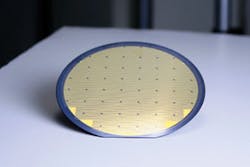
Currently Nitronex deposits GaN on 4-inch silicon wafers, although work is in progress to move up to 6-inch diameters. The silicon wafers begin with standard 500- to 525-micron thickness, but are thinned after processing to 150 microns. New designs call for a 100-micron thickness. The GaN film on top of the wafer is only about 2 microns thick.
One of the problems that must be solved during the deposition of GaN onto a silicon chip is the difference in coefficient of thermal expansion between the two materials. Nitronex solves this problem during processing-the details are proprietary-and the GaN film remains firmly bonded to the silicon substrate through thousands of thermal cycles.
The fact that GaN-on-silicon is 99 percent silicon has an obvious implication for using a small GaN-on-silicon die as a chiplet inserted into a larger silicon die. “Our chip is essentially a silicon chip,” Piner observes. “So when it comes to the laying of a chiplet in a larger CMOS silicon chip, the TCE that our chip is going to experience is the same as the chip that it is being implanted into.”
There is another way to take advantage of GaN-on-silicon, and that is by processing the GaN circuitry on only part of the die, then etching off the GaN film (which is only 2 microns thick) from the rest of the die and continuing with normal silicon processing. The result would be GaN functionality (a power amplifier, for example) and processing functions on the same chip.
A key objection to mixing GaN and silicon is that gold is the established material of choice for vias and other structures in GaN chips. In a silicon fab, gold is considered poison. “The easiest thing to do-and this is something that is actually already under way-is to take the gold out of the GaN or out of the III-V process in the first place,” Piner says. “I know devices operating today, using GaN on silicon, that have been processed basically in a silicon fab-no gold anywhere in it-and they get as good a contact as we can get. If you have the process capability, if you have the resources and the brain power, it’s not that difficult a problem to tackle.”
Gold aside, there are other considerations involved in putting GaN and silicon functionality on the same wafer, but Piner has good reason to think this can be done. “I’ve actually worked out the details in two different instances with university institutions, with regard to doing a CMOS process and a GaN process on the same wafer,” he explains.
“We have come up with process flows that would work and stay within the thermal budget of the CMOS process and not subject the GaN to any undue chemicals or treatments or anything of that nature that would concern you in terms of creating problems for the GaN device operation.”
The two separate approaches-using silicon and GaN processing on the same chip, and inserting chiplets of a dissimilar material-mean that it should be possible to create multichip module-type assemblies at the chip level-a real system on a chip, Piner notes. The obvious benefits are great reductions in size and weight, along with the options of improved functionality.
Piner points out that such assemblies are not likely to happen soon; five years, he thinks, might be a reasonable timeframe, especially if development is driven by the need for smaller and lighter communications and radar systems.


