IC bonding technology will enable design engineers to stack semiconductors—not scale them—to improve the performance of image sensor arrays
By Chris Sanders
As military and aerospace design engineers develop imaging systems for the wired battlefield of tomorrow, they face the challenge of providing high-resolution imaging arrays that are light, small, and cheap, yet that can deliver the high resolution necessary for imaging systems ranging from surveillance cameras in unmanned aerial vehicles (UAVs) to satellite imaging systems, to infrared night-vision goggles.
In the commercial semiconductor industry, chip makers continually look for new ways to shrink the sizes of their devices. The traditional path of commercial semiconductor development has been to thin-down line widths for integrated circuits (ICs)—from 1.25 micrometers, to 90 nanometers, to 45 nanometers, and down to today’s 32 nanometers nodes and beyond.
With each step down in IC scaling, however, the development costs increase exponentially and the technical challenges get harder to solve. The primary drivers for 3D integration in the commercial arena involve increasing the interconnection density (the ability to pack more transistors and more functionality onto an IC), optimizing manufacturing yields (ensuring that high volumes of semiconductor wafers can be processed efficiently with few defects), and reducing costs (which relates to manufacturing yields in that more wafers can be produced more cost effectively in a given production cycle).
While these factors also have an influence in the development process for military and aerospace semiconductors, the primary advantage of 3D IC integration for imaging sensors in defense electronics is the ability to achieve high-performance imaging arrays using proven and less costly IC technology (i.e., 90 nanometers and higher).
Backside illumination
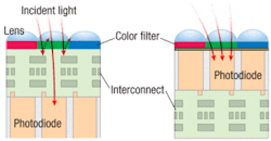
In a traditional CMOS imaging sensor array, the image sensor is a matrix of photodiodes and color filter elements designed to capture light (photons), and the control circuitry is formed on a layer above this matrix. Using this front-side illumination (FSI) technique, a portion of the light that should enter the image sensor is refracted, blocked, or otherwise distorted by the metallized dielectric elements of the control circuitry, thus reducing the image sensor’s performance.
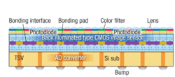
Using a back-side illumination (BSI) design moves the control circuitry to the reverse side of the chip containing the photodiode/lens/filter array, and thus enables 100 percent of the image sensor to be used for light capture. Implemented through the use of 3D IC integration, this type of BSI architecture delivers reduced pixel size, increased low-light sensitivity, enhanced quantum efficiency and reduced cross talk, which in turn lead to significant improvements in sensor performance and image quality, as well as reduction in cost. BSI technology provides superior low-light sensitivity and enables flatter lenses to be used, which makes for thinner camera and image sensing modules.
Vertical interconnections
Because the processing steps are different for the sensor array wafer and the control circuitry wafer, it is necessary to find a way to join the separately-processed elements together, electrically and mechanically. There are three enabling technologies critical to the ability to stack semiconductor layers and form the structures necessary to produce a multi-layer design required to implement a next generation BSI CMOS image sensor.
Because they are built a few microns into the silicon substrate and do not impede the conventional interconnect routing, these TSVs are easily scalable. When the wafers are thinned to reveal the TSVs, they can either be bonded “as is,” or a bonding metal, such as nickel, copper, or other suitable material may be patterned on top of the revealed TSV and planarized (made smooth) with oxide deposition and CMP in preparation for bonding. TSVs can also be formed after the primary IC processing is completed by etching through the wafer layers to expose metal columns that extend through the backside of the wafer.
The second enabler is wafer thinning technology. To implement BSI designs, typically the wafer carrying the photodiode arrays must be thinned to expose the interconnects (TSVs) on the device’s backside prior to bonding. Wafer thinning typically involves mechanical grinding of the wafer’s back surface, and/or chemical polishing to produce a smooth surface. For silicon wafers with embedded metal, it is important to consider that the bonding metal, especially copper, is typically softer and more ductile than the surrounding silicon and the polishing process can result in “dishing” or a non-planar surface, which complicates bonding.
The third enabling technology is a reliable, low-cost wafer bonding process, which is the most technically complex challenge for semiconductor manufacturers to overcome. The ideal bonding technology would be scalable for 3D interconnect for either wafer-to-wafer or die-to-wafer fabrication processes.
Different approaches to bonding
The challenge of developing a reliable, repeatable, low-cost bonding technology has resulted in three different methods for wafer-level bonding today: 1) Metal-to-metal thermocompression bonding; 2) Conductive and non-conductive polymer adhesives; and 3) Direct oxide bonding (also known as “fusion,” “covalent,” or “molecular” bonding). Each of these processes has both advantages and limitations for BSI CMOS imaging sensors.
Thermocompression bonding
Metal-to-metal thermocompression bonding has been the preferred technology for early efforts in 3D IC integration; experts prefer it because it forms mechanical and electrical interconnections simultaneously. This process bonds the exposed metal surfaces of previously formed TSVs with temperatures from 350 to 450 degrees Celsius, as well as 30 minutes under pressure.
This process has its drawbacks. Elevated temperature limits the alignment accuracy of most thermocompression processes to 1.8 to 2 microns. In addition, the need for separate temperature and pressure chambers to complete the bonding process adds significant processing time, which directly influences processing costs. High temperatures and pressure on CMOS imaging sensors also can distort the image sensor elements of the wafer.
Polymer adhesives
Another technology that has been used for 3D IC integration involves applying conductive and non-conductive polymer adhesives to different wafer levels, aligning the wafers, and placing them in specialized process chambers for curing. This approach can require 30 to 60 minutes per wafer, and as many as four process chambers, with a throughput capacity of four to eight wafers per hour in each chamber. Current alignment technology limits the bonding accuracy to 1.8 to 2 microns, which can affect yields and increase processing costs.
Direct oxide bonding
Employing direct oxide bonding (also referred to as “covalent” or “molecular” bonding) creates vertical metal-to-metal interconnection between wafer layers with non-conductive heterogeneous oxide (SiO2) to activate chemical bonds between exposed conductive materials on each wafer’s surface. By preparing the planarized wafer surfaces with the oxide, the formation of chemical/molecular bonds is enabled at significantly lower temperatures, thus eliminating the high temperature and pressure.
To achieve 3D IC stacking, experts planarize the top and bottom of the wafers before bonding to expose the metal TSV interconnections. The topside contacts are bonded to the backside, which has been thinned to expose the bottom of the next layer TSVs or topside of the next level wafer. Alternatively, wafer surfaces can be prepared by seeding a metal layer on top of the TSV structures, then depositing an oxide layer.
Nickel is often used for this metal layer, since its hardness facilitates the CMP (chemical-mechanical planarization) process. Copper can also be used, however; adjustments to the CMP process are required to mitigate “dishing” that can otherwise occur as the softer copper undergoes CMP. When the surface is flattened through CMP processing to expose the TSV metal and SiO2 coplanar surface, the room temperature bonding process can occur.
The bonded structures may then be heated for a short period to reinforce and enhance the 3D interconnections. The optimum temperature depends on which bonding metal is used. For example, nickel may need heating to about 300 degrees C, while copper will only require about 150 degrees C or less to form monolithic low-resistance metal-to-metal interfaces. The activated and terminated oxide layers bond with sufficient energy to generate internal pressure when the DBI metal expands with the increase in temperature to form a reliable metallic bond to complete the interconnection.
The advantages of direct oxide bonding include processing time per wafer of three to six minutes, and increased alignment accuracy; current technology enables bond accuracy to within 1.2 microns, with improvements expected to tighten that to 0.5 microns or better. In addition, it is possible to achieve several layers of integration using direct oxide bonding without compromising yields. More importantly for CMOS imaging sensors, the direct oxide bonding process does not create additional distortion in the finished focal plane array.
Another significant advantage is the option of using more established and often less expensive 1.25-micron or 90-nanometer semiconductor technology for the sensor control circuitry, without compromising performance, density, or cost.
Application to military imaging
The ability to place the entire signal processing circuitry directly on the active side of a CMOS wafer enables g improved processing speeds as well as reduced manufacturing costs by allowing the use of older and less expensive CMOS technology. Another benefit is dedicating 100 percent of the surface area of the pixilated sensor array, to image capture, which improves resolution and creates a compact, high-performance sensor.
Military applications of this technology include UAV guidance and surveillance cameras; satellite imaging systems; airborne imaging systems; infrared imaging systems, such as missile guidance, night-vision, and security systems; millimeter-wave radar; and remotely deployed or soldier-carried battlefield cameras.
Chris Sanders is director of business development at Ziptronix Inc. in Morrisville, N.C., which specializes in 3D semiconductor manufacturing. Learn more about the company online at www.ziptronix.com.
More Military & Aerospace Electronics Current Issue Articles
More Military & Aerospace Electronics Archives Issue Articles


