- Reconfigurable Xilinx® Artix®-7 FPGA
- 48 Digital I/O
- 20 Diff or 40 SE Analog Inputs
- 16-bit ADC
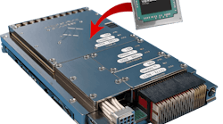
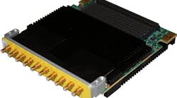
XMC-7A50-AP323 XMC Module with Artix®-7 FPGA and High-Density I/O Description
XMC-7A50-AP323: 48 TTL channels Custom Requirements: Other I/O combinations are possible, contact Acromag for more information. Build Option A: 24 EIA-485/422 channels Build Option B: 24 TTL and 12 EIA-485/422 channels Build Option C: 24 LVDS channels
Designed for COTS applications, these XMC modules combine a user-customizable FPGA with digital I/O and high-performance analog inputs for high-density signal processing.
The XMC-7A50-AP323 series provides a FPGA based user-configurable bridge between a host processor and a custom digital interface via PCI Express. These XMC boards feature a best-in-class Artix®-7 interface to deliver the industry’s lowest power and high performance.
The analog inputs monitor 20 differential or 40 single-ended channels. Software or an external hardware input can trigger A/D conversions for synchronization to external events. On-board, precision voltage references enable accurate software calibration of the module without external instruments.
The Engineering Design Kit provides users with basic info. required to develop custom FPGA firmware for download to the Xilinx® FPGA. Example FPGA design code is provided as a Vivado IP Integrator project for functions such as a one-lane PCI Express interface, DMA, digital I/O control register, and more. Users should be fluent using Xilinx Vivado® design tools.
Key Features & Benefits
FPGA Digital I/O
· Reconfigurable Xilinx FPGA
· High channel count digital interface: TTL, RS485, and LVDS interface options
· 32Mb quad serial flash memory
· 52,160 logic cells
· 65,200 Flip flops
· 2,700 kb block RAM
· 120 DSP slices
· External LVTTL clock input
· Long distance data transmission
· Example design
· Power up and system reset is failsafe
Analog Input
· 20 differential or 40 single-ended inputs
· Flexible scan control
· 16-bit A/D resolution
· 8μs conversion time
· FIFO buffer with 16K sample memory
· Interrupt upon FIFIO threshold condition
· FIFO full, empty and threshold reached flags
· Programmable channel conversion control
· Programmable conversion timer
· Several scanning modes
· External trigger
General
· Wide temperature range
· Conduction cooling options
· Software development tools for VxWorks®, Linux®, and Windows® environments
Performance Specifications
XMC Compliance
Complies with ANSI/VITA 42.0 specification for XMC module mechanicals and connectors.
Complies with ANSI/VITA 42.3 specification for XMC modules with PCI Express interface.
Electrical/Mechanical Interface: Single-width module.
PCI Express Base Specification
Conforms to revision 2.0
Lanes: 1 lane in each direction.
Bus Speed: 2.5 Gbps (Generation 1).
Memory: 128k space required. 1 base address register.
FPGA
FPGA device: Xilinx Artix-7 FPGA Model XC7A50T.
FPGA configuration: Download via flash memory.
Example FPGA program: IP integrator block diagram provided for PCIe bus 1 lane Gen 1 interface, DMA controller, on chip block RAM, flash memory and control of field I/O. See EDK kit.
I/O Processing
Field I/O Interface: PCIe bus 1 lane Gen 1 interface.
I/O Connector: 100 pin field I/O connector.
Engineering Design Kit
Provides user with basic information required to develop a custom FPGA program. Kit must be ordered with the first purchase of a XMC-7A50-AP323 series module
(see www.acromag.com for more information).
Digital I/O
TTL Channels
48 input/output channels. Direction is controlled in groups of eight channels. 5V tolerant.
TTL Electrical Characteristics
VIH: 2.0V minimum.
VIL: 0.8V maximum.
IOH: -32.0mA.
IOL: 64.0mA.
VOH: 2.0V minimum.
VOL: 0.55V maximum at 64mA.
Analog Input
Input configuration: 20 differential or 40 single-ended.
A/D Resolution: 16 bits.
Input range (dip switch-selectable)
Bipolar ±5V or ±10V.
Unipolar 0 to +5V or 0 to +10V.
Data sample memory: 16K sample FIFO buffer.
Maximum throughput rate: 200KHz (5μS/conversion).
A/D triggers: External, and software.
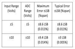
System accuracy: 2.4 LSB (0.014%).
Maximum overall calibrated error at 25°C.
Data format: Binary two’s compliment and straight binary.
Input overvoltage protection: Power on: -20V to +40V. Power off: -35V to +55V
Common mode rejection ratio (60Hz): 96dB typical.
Channel-to-channel rejection ratio (60Hz): 96dB typical.
Environmental
Operating temperature: -40 to 70°C.
Storage temperature: -55 to 100°C .
Relative humidity: 5 to 95% non-condensing.
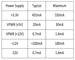
Power
Physical
Length: 5.866 inches (143.75mm.)
Width: 2.9134 inches (74mm.)
Weight: 3.392 oz (96.162g).