CONCORD, Mass. – U.S. military microelectronics experts plan to build a 161,000-square-foot advanced compound semiconductor laboratory and microelectronics integration facility for multi-wavelength sources, large-format multi-wavelength detector arrays, RF and microwave electronics, high-power electronics, and integrated photonics.
The new microelectronics facility will be at Hanscom Air Force Base in Bedford, Mass., and is to enable the Massachusetts Institute of Technology Lincoln Laboratory to apply advanced technology to problems of national security.
Officials of the U.S. Army Corps of Engineers New England District in Concord, Mass., announced a $278.6 million contract Thursday to the Gilbane-Exyte joint venture in Providence, R.I., to build an advanced compound semiconductor laboratory and microsystems integration facility at Hanscom Air Force Base.
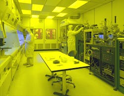
The compound semiconductor facility at Hanscom Air Force Base will consist of new laboratory and office space with a cleanroom complex for use by the Lincoln Lab Advanced Technologies Division.
The facility will have about 90,000 square feet of cleanrooms; 52,638 square feet of microsystem integration cleanrooms; 12,000 square feet of building support; and 7,000 square feet of physical plant.
The intent is to consolidate Lincoln Lab's existing compound semiconductor materials growth, fabrication, and characterization facilities to enable multi-wavelength sources, large-format multi-wavelength detector arrays, radio frequency electronics, high-power electronics, and integrated photonics fabrication and packaging of specialized advanced electronic prototypes.
The new facility will be three stories high and will include large and sophisticated cleanrooms for microprocessor development and experimentation; complex heating, cooling, and electrical systems; secure communications areas; places for hazardous, toxic, and corrosive process liquid and gas; transport, distribution and waste collection systems; and a foundation that minimizes vibration and noise.
In addition, the facility will have new will have new access roads, replacement parking, utilities, and landscaping. For more information contact Gilbane Building Co. online at www.gilbaneco.com, MIT Lincoln Laboratory at www.ll.mit.edu, or the Army Corps of Engineers New England District at www.nae.usace.army.mil.


