USC, DARPA zero-in on technologies for high-end military integrated circuit (IC) custom design
Officials of the U.S. Defense Advanced Research Projects Agency (DARPA) in Arlington, Va., announced AN $8.2 million contract modification Tuesday to the USC Information Sciences Institute (ISI) in Los Angeles for phase-two options in the Circuit Realization at Faster Timescales (CRAFT) – FinFET Foundry/Design Aggregation Services military chips program.
The CRAFT FinFET program seeks to develop a custom IC design flow to reduce the effort necessary to design high-performance custom ICs; help port IC designs to secondary IC foundries and more advanced technologies; and reuse of IC intellectual property.
USC ISI won an $11.8 million contract in December 2015 for the first phase of the CRAFT FinFET program. USC ISI then won $3 million in CRAFT FinFET contract options in March 2016 -- $1.2 million for phase 1, $890,524 for phase 2 option 1, and $840,335 for phase 3 option 2.
To maintain technology dominance, the U.S. military is developing next-generation systems that require high computational performance in a power-constrained environment. The problem, however, is these technologies cannot be manufactured fast enough. Systems designers today must choose between high performance and low power consumption.
Related: COTS designers turn to Hybrid packaging
For the most crucial applications, systems designers must choose between a high performing, custom ICs that requires years to design and fabricate, or settle for a 100-times lower-performing general-purpose processor that can be programmed in months.
The DARPA CRAFT program seeks to demonstrate a custom IC design flow and methodology in a leading-edge commercial 16- or 14-nanometer fab, port these designs to new foundry process flows, and increase design reuse by providing a repository for secure storage and distribution of design elements.
The CRAFT has three technical goals: reducing custom IC design and fab cycle time by 10X with new software tools; enabling a 50 percent reuse of critical military IC modules with an intellectual property (IP) repository system; and enabling flexible chip fabrication by porting a technology node from one foundry to another, or migrating from one design node to another design node at the same foundry.
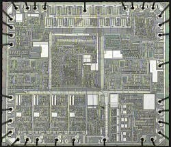
To meet these goals, DARPA needs to build custom ICs using the FinFET leading-edge CMOS process node because of this technology's density, performance, and power advantages. To access this technology, the CRAFT program needs FinFET foundry access, and this is where USC Information Sciences Institute comes in.
Related: DARPA to revolutionize high-end IC design for military and aerospace uses
In the program's first phase USC experts will have demonstrated a 10X reduction in design efforts using a standard flow for a system-on-chip (SoC) with logic block size of more than 200,000 gates; several mixed signal blocks, SRAM memory blocks, and third-party intellectual property (IP) blocks.
In the second phase, USC experts will demonstrate a 7X reduction in design efforts to create a DARPA-selected SoC design, document the design flow; test fabricated chip functionality across standard temperature ranges; characterize an initial suite of macros and generators; document a reference CAD flow; and design a suite of macro and generators.
USC is providing a design aggregation service for other CRAFT contractors as they perform dedicated and foundry-driven FinFET multi-project wafer (MPW) shuttle runs. USC Information Sciences has prior experience in working with leading-edge technologies, and will act as the primary interface between the foundries and DARPA.
On this contract modification USC ISI will do the work in Marina Del Rey, Calif., and should be finished by August 2018. For more information contact the USC Information Sciences Institute online at www.isi.edu, or DARPA at www.darpa.mil.
Learn more: search the Aerospace & Defense Buyer's Guide for companies, new products, press releases, and videos
