Test and measurement for finding defects in high-voltage multi-layer ceramic chip capacitors (MLCCs)
Repeated thermal cycling can cause an air gap to generate a crack extending into the dielectric layer adjacent to the gap. With further thermal cycling, the crack will lengthen, and often expand into several crack defects. When a crack reaches the next electrode, a conductive or leakage pathway has been formed between two electrodes. The high voltage typically causes the MLCC not merely to fail but to explode -- with undesirable consequences. The same failure mechanism causes lower-power MLCCs to fail, but without as much force.
Since high-voltage capacitors consist largely of many alternating layers of electrode and dielectric, there are obviously many locations where gaps can occur. In any life- or mission-critical application, it is important to exclude from usage high-voltage MLCCs having such defects. Thin gaps -- those a tiny fraction of a micron in size -- can be just as dangerous as much thicker ones.
MLCCs have far more material layers and material interfaces than there are in an integrated circuit package, an isolated gate bi-polar transistor (IGBT), or a flip chip, yet the ultrasonic pulse can travel through the whole thickness of an MLCC; it can have dozens or even hundreds of layers, be reflected from the bottom-most interface, and sail back to the transducer with an image to deliver.
Related: Optical revolution prompts a search for new military connectors
Making the acoustic images illustrating this article were C-SAM acoustic micro imaging tools in the Nordson SONOSCAN laboratories in Elk Grove Village, Ill. The tool’s transducer travels at high speed, while scanning samples. It performs several thousand pulse-echo sequences per second, each at a defined X-Y location. If the pulse encounters only electrode-to-dielectric interfaces, it produces no distinct large echoes, and the pixel for that location will be black. If it encounters a solid-to-air interface, the pixel will be bright white or a selected pseudo color, usually red.
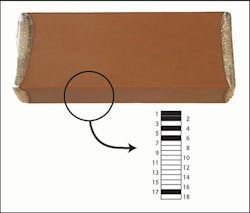
Echoes from interfaces near the top of the MLCC arrive at the transducer first, while those from near the bottom arrive last. For the MLCC shown here, the whole time span during which echoes might arrive from a pulse was divided into 18 parts, so each echo could be imaged in its assigned gate. Viewed in sequence, the gate images will show not only the internal features but also the respective depths of those features. Scanning 18 gates, or even more, takes the same time as scanning one gate, but produces several images.
The MLCC imaged was 1.8 centimeters long, 7.6 millimeters wide, and 3.8 millimeters thick. Each of the 18 gates is thus about 210 microns thick, and is probably several times thicker than individual dielectric or electrode layers. The C-SAM tool performed imaging at a frequency of 30 MHz. Most gates did not reveal any defects. The four gates whose acoustic images are shown here are highlighted in Figure 1.
Related: Revised moisture sensitivity standard includes lead-free components
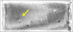
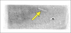
A few small features are visible in Figure 2. Each is surrounded by a sort of halo (arrow). The halos suggest that these are features such as irregularities on the surface of the capacitor, and not internal features. They lie outside the gate but are being imaged as acoustic shadows by ultrasound returning from below. The much larger indistinct dark gray features are acoustic shadows caused by variations in the flatness of the part’s surface. There are no significant internal features within Gate 1 itself.
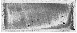
In Gate 2 (Figure 3), there are a few circular features of various diameters. The shape suggests that they are spherical or pancake-shaped air-filled voids and that they lie mostly or entirely within Gate 2. Gap-type features such as these can generate the cracks that cause, for example, a communications system to fail. Less distinct circular features may lie partly within Gate 3.
Related: Rad-hard moves into the submicron age
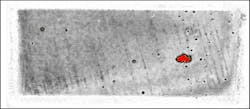
In Figure 4 (Gate 4) the landscape suddenly changes dramatically. There are about two dozen small voids within this gate, as well as one large void pseudo colored red. The large void may be limited in its upward movement by one layer within the capacitor that caused most of the void’s interface area to appear red. It may have formed during processing from the merging of two or more smaller voids. The numerous smaller voids probably formed at the same interface, but they are too small for any color to be visible.
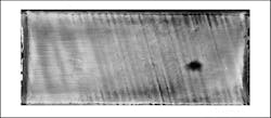
There are almost no features of interest below Gate 6, but a feature of interest is imaged by the echoes from Gates 17 and 18. Gate 17, the sharper of the two, is shown in Figure 6. The dark feature right of center is the acoustic shadow of the large void in Gates 4 and 5 above. It formed in this way: Ultrasound pulsed by the transducer was locally blocked by the void in Gate 4 and did not reach the bottom of the capacitor. Ultrasound was reflected from all other areas of the bottom, but not from the area of the acoustic shadow. When reaching the transducer, the lack of echo signals created the acoustic shadow.
This article has examined anomalies within one high-voltage MLCC, and at their specific depths. These anomalies, even if minuscule, are capable of causing instantaneous failure of the high-voltage MLCC and impairment or failure of the system they are part of. But the solid-to-air interface of these anomalies reflects virtually 100 percent of an ultrasonic pulse and makes them highly visible. Capacitors displaying these features should be prevented from being used in navigation systems, warning systems and numerous other critical applications in order to guarantee overall performance reliability.
Tom Adams is a consultant for Nordson SONOSCAN Inc. in Elk Grove Village, Ill. Contact him by email at [email protected].
Ready to make a purchase? Search the Military & Aerospace Electronics Buyer's Guide for companies, new products, press releases, and videos
