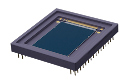
Teledyne e2v releases CIS120 CMOS imaging sensor for space and harsh environments
CIS120 has been designed as a general purpose imager for space applications. Back-illumination, combined with low readout noise and on-chip analogue-to-digital conversion give excellent image quality. Pixel read timing is set by an on-chip sequencer to simplify use and to reduce pin count. A column parallel ADC is used to quantise each row of pixels in turn and is controlled by its own sequencer. Resolution can be set from 8 to 14 bits.
Four LVDS channels output the image data and are controlled by the readout sequencer to scan along each row in turn. Two LVDS synchronisation channels allow accurate data sampling.
All configuration settings are programmed over an SPI. This includes shutter mode, ADC resolution and bias current values. Package options will range from a ceramic PGA to metal and ceramic three-side buttable designs for use in mosaic focal planes.
The sensor configuration registers control all imager settings (including shutter mode, ADC resolution and bias values) and are programmed through an SPI interface. The pixel access is per row and driven by an on-chip pixel sequencer with separate row decoders for left and right halves of the pixel array.
The analogue pixel outputs are converted to digital values by a column parallel ADC with programmable resolution (8 to 14 bit). The digital words are stored in a register bank until serialised and output through the four LVDS data interfaces, with two LVDS for synchronisation. Readout timing is controlled by the on-chip readout sequencer. Frame rate is determined by ADC resolution, shutter mode and the use of ROI.
A programmable PLL can be used to generate the 130 MHz clocks for the ADC and the data output, from a range of external reference frequencies.
An on-chip programmable biasing block generates all required analogue bias currents from only four input reference currennts and so helps to minimise the number of pins. For m ore information, please visit https://www.e2v.com/resources/account/download-datasheet/3664.

