Optical switching: the military passes on photonics but industry grabs the MEMS ball
Military technology leaders are shelving government photonics research, and are relying on an ever-robust commercial industry to speed the flow of data by converting electrons into light
By John Rhea
After a decade of military-sponsored research, optical computing as the successor to conventional electronic information processing remains as elusive a goal as ever. Instead, the focus has shifted to commercial efforts in optical switching, which are yielding powerful tools to convert electronic computer data into photons for optical fiber networks of ever-increasing bandwidth.
Driving this shift are the mounting demands of the telecommunications industry in this age of the Internet. Switching capability, as measured by the American National Standards Institute (ANSI)-sponsored standards for the Synchronous Optical Network (SONET), has risen from 2.5 gigabits per second for the OC-48 standard to 10 gigabits for the OC-192. The next step is 40 gigabits for what is informally being called OC-768 (four times 192) pending its approval as an ANSI standard.
Bell Labs, the research arm of Lucent Technologies based in Murray Hill, N.J., last year took a series of steps to achieve this goal — and go beyond it — with optical switches incorporating one key military-sponsored technology, micro-electromechanical systems (MEMS). Now, with other companies likely to follow Lucent`s lead, military users are in a position to take advantage of the new generation of commercial optical switches — and, in the process, get some dividends from the investment by the Defense Advanced Research Projects Agency (DARPA) in pioneering MEMS technology.
In introducing the new switch at the Optical Fiber Communications conference last year in San Diego, David Bishop, head of the Bell Labs microstructure physics research department, described MEMS as "a disruptive technology — one that changes the paradigm for an entire industry" — and the basis for the switching technology of future optical networking systems.
Electronics experts fabricated MEMS devices in much the same way as silicon integrated circuits, Bishop explained. They deposit and pattern various films, such as polysilicon, silicon nitride, silicon dioxide, and gold to produce multilayer, three-dimensional structures. The major difference is a step at the end of fabrication in which they remove some of the materials using a selective etching technique that leaves the devices with movable elements — hence the "mechanical" part of MEMS.
The switch is thus a pivoting bar with a gold-plated mirror on one end. This mirror fits between two optical fibers lined up end to end. When the switch is off, the mirror rests below the cores of the two fibers, allowing photonic signals to travel from the core of one to the other. Turning the switch on applies a voltage at the other end of the bar to lift it so that the mirror reflects the light rather than letting it move from one fiber to the other.
Among the applications that Bishop envisions are optically reconfigurable communications networks, power limiters, variable attenuators, and wavelength-division multiplexed (WDM) signal equalizers.
Lucent officials followed up that disclosure the following month with the introduction of what they call the WaveStar 40G express single-laser optical transmission system: 40 gigabits per second over a single wavelength using time division multiplexing (TDM). MCI WorldCom at its Richardson, Texas, network technology laboratories tested the prototype system at distances as far as 100 kilometers using standard fibers. Lucent had previously demonstrated an 80-channel dense wave division multiplexing (DWDM) system; the stage was set for putting the two technologies together into an operational commercial system
That happened in November with the introduction of Lucent`s LambdaRouter optical switch based on WaveStar MEMS technology. This approach features 256 mirrors fabricated on an area smaller than one square inch of silicon, each capable of achieving the bandwidth of the proposed 40-gigabit SONET standard. Deliveries to selected customers are due to begin by mid-year of units with total switching capacities up to 10 terabits (trillion bits) per second, and the system will be commercially available in December, Lucent officials claim.
This technology is expected to evolve and soon be available to military users. Still to be resolved, however, are power density issues. Transmitting data over a single wavelength requires only microwatts of power, but power becomes more troublesome at 256 wavelengths. This leads potentially to nonlinearity that could shrink the distance between repeaters in end-to-end systems and require more amplifiers.
Engineers at the Raytheon Tactical Systems division in Fort Wayne, Ind., reported a military application of MEMS last month. This application uses the technology in a frequency-agile filter that delivers 25 watts at very high frequency (VHF) to tune the filter`s output.
The implication of this could be an interference filter for the U.S. Army`s Joint Tactical Radio System (JTRS) to minimize interference among transceivers operating in close proximity. The technology also may enable users to harness the full power of their programmable digital radios, says Ken Peterman, Raytheon`s business development director.
In this application MEMS relays enable designers to build filter-tuning circuit boards that are half the size of filters using conventional PIN diode switches, Peterman notes. They also offer the promise of increasing the typical power efficiency of radio frequency (RF) amplifiers from 30 percent to 80 percent. Increased power efficiency translates into reduced battery and cooling requirements. Experts at Cronos Microsystems supplied the MEMS relays used in these tests in Research Triangle Park, N.C., which also serves consumer and industrial markets.
As previously reported, scientists at Silicon Light Machines in Sunnyvale, Calif., used what they called "optical MEMS" to create "switchable pixels" that would produce maps, intelligence data, command and control, and other tactical displays. DARPA officials sponsored this work, and considered it to be scaleable because it is inherently digital and can be manufactured with conventional silicon-based processes using commercial foundries to fabricate the wafers.
This is a technology based on grating light valves (GLVs), originally developed at Stanford University in Palo Alto, Calif. GLVs should find commercial markets in parallel with the military applications. By using a bright light source such as a metal halide or xenon arc projection lamp, GLV devices can act as display engines for large projection systems and, at the other end of the spectrum, the low power systems that military designers need.
These are modest steps that fall short of the pivotal role envisioned for photonics a decade ago, when the Air Force identified it as the single most important technology in changing the way the service performed its missions of the 21st century.
The Air Force Research Laboratory`s Photonics Center in Rome, N.Y., had that responsibility. Yet Air Force leaders have replaced this facility with two branches — Photonics Processing and RF Photonics. These activities are at the bottom of the organization chart for the laboratory`s Sensors Directorate (now headquartered at Wright-Patterson Air Force Base in Dayton, Ohio). DARPA officials, meanwhile, are phasing out their ultra-photonics effort within its Microsystems Technology Office after 10 years.
In the process, government officials have deferred the search for general-purpose optical computing in favor of more immediate incremental improvements. One of the two remaining branches at Rome, for example, works on photonic modules for multimode RF signals and sensors necessary for radar, electronic warfare, and communications systems. The other concentrates on interconnects and memories for automatic target recognition and command and control functions.
The use of optical switches as the intermediary between the electronic functions that take place within the black boxes and the fiber optic networks that interface with the real world thus becomes the model for further expansion of photonics in both directions: toward the digital world of optical processing and the analog world of sensor functions. The military traditionally has to pay for sensor development itself since there is little overlap with commercial markets. Yet leaders in the semiconductor industry already envision a time — 20 years at best — when the "gods of physics" will not permit any further reduction in the sub-micron feature sizes of electronic switching elements.
What military-sponsored optical computing research has accomplished to date is defining a digital system architecture like electronics that would not need switches that are vulnerable to heat dissipation. Instead, the laser diodes in the photonic devices would emit a continuous beam of light that could turn at right angles to perform the switching function. For example, the beam could be turned to the left to represent a "one" and to the right for a "zero."
The same criteria that made photonics the Air Force`s top technology priority a decade ago remain valid today: orders of magnitude improvements in processing power and bandwidth, immunity to electronic countermeasures, greater stealth due to the elimination of telltale electromagnetic radiation, reduced weight and power (critical considerations in airborne systems), less heat-induced damage to fragile components, and — ultimately — lower costs.
BMDO funds optical switch for dual-use application
ALEXANDRIA, Va. — A newcomer to optical processing for military applications is the Ballistic Missile Defense Organization (BMDO) in Arlington, Va. BMDO leaders, in parallel with the telecommunications giants, are funding research to develop optical switches and move closer toward the goal of totally photonic networks.
BMDO is sponsoring Chorum Technologies Inc. of Richardson, Texas, in an effort to apply liquid crystal technology to an all-optical switch that would eliminate the need for bandwidth-limiting electro-optical signal conversions and simplify the process of routing data traffic through high-capacity fiber optic networks.
Chorum engineers are conducting the work under terms of a small business innovative research (SBIR) contract in an attempt to develop optical networks that operate in the terabit (trillion bits) range. The use of liquid crystals has cut crosstalk to less than -60 decibels and insertion loss to less than -1.5 decibels, according to BMDO. Liquid crystals also reduce power consumption and permit polarization-insensitive operation and millisecond-to-microsecond response times regardless of the operational temperature.
The project is part of BMDO`s stress on dual-use technology. The organization reports that Chorum has begun to commercialize the product as part of a family of products that also includes multiplexers, demultiplexers, processors, and integrated systems. Sampling has begun, and commercial shipments are due to begin by year`s end. — J.R.
DARPA, AFOSR sponsor terabit optical memory using dye lasers
MENLO PARK, Calif. — Scientists at SRI International in Menlo Park, Calif., are using conventional semiconductor processing techniques and dye lasers in what they call a coherent time-domain optical memory (CTDOM). Experts say CTDOM may achieve storage densities of a trillion bits per cubic centimeter and data rates of more than 10 gigabits per second.
The work aims at developing high-density random memories capable of storing two-dimensional images for a variety of military and commercial applications. Funding the work is the Air Force Office of Scientific Research under supervision of the Defense Advanced Research Projects Agency in Arlington, Va.
Fabrication starts with an inert crystal silicon host doped with rare-earth impurity ions such as Europium on which data are stored. The laser pulses illuminate the ions, which see the pulses as either in or out of phase, thus permitting digital operation.
The SRI experiments to date have stored 500 wavelength-multiplexed holographic images, each consisting of 512 by 488 pixels, at the video frame rate of 30 cycles per second. Using a spatial light modulator with a laser peak power of seven milliwatts, a single frame could be stored in less than 75 microseconds. Team members now say they can achieve recording/retrieval rates greater than 14,000 frames per second. — J.R.
Universal chassis mixes and matches multimode, single mode fiber optics
CHATSWORTH, Calif. — The multiplicity of optical communications formats dictates the need for a universal chassis. This would enable users to mix and match their hardware, maintains Don Bouchard, vice president and general manager of data communications products at Canoga Perkins, in Chatsworth, Calif..
Company officials last October introduced a family of fiber optic converters that convert short-haul multimode signals to long-haul single mode signals without optical multiplexing.
This is particularly important for secure and encrypted military communications, he says. This could enable systems designers to convert data in an electrical format using frequency division multiplexing (FDM) to an optical format for wavelength division multiplexing (WDM). "WDM is just optical FDM," Bouchard quips, and the idea is to get everybody on the same page.
Using the company`s universal chassis, the customers can combine T-1 lines, local area networks, modems, multiplexers, and converters into one system under their control. The security feature is reflected in increased use of the Canoga Perkins systems during overseas crises by the White House and the "Maryland Procurement Office" (the euphemism for the National Security Agency in Fort Meade, Md.). Security is so tight at the latter, he says, that company personnel are limited in their access to service the equipment.
The latest enhancement to the universal chassis of Canoga Perkins is what is known as the L6xx family of fiber optic converters in either a rack-mounted or stand-alone configuration. This setup converts an input optical signal to a different or repeated output optical signal at either the standard 1,310 or 1,550 nanometer wavelengths.
There are compelling reasons for the use of fiber optics instead of electrical cabling or broadcasting in certain hostile military environments, according to Bouchard. These include reduced vulnerability to interception, jamming, and revealing the locations of the users. —J.R.
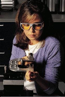
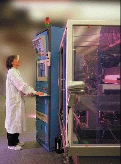
A battery of sophisticated tests at the Corning optical technology facility is key to maintaining quality, reliability, and speed of optical switches. U.S. military leaders are taking advantage of commercial optical technology development for the latest defense and aerospace systems.
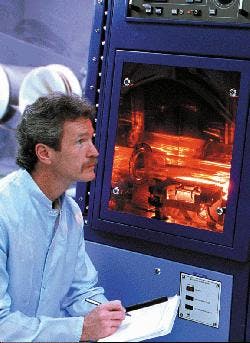
An optical fiber technician from Corning pays close attention to test data that will help him fine-tune optical components necessary for today`s optical switches.


