Copper-post technology shows promise for cooling in military applications
By Keith Gurnett and Tom Adams
A few months ago the Canadian reverse-engineering firm ChipWorks announced that Intel was using copper posts instead of solder bumps in its latest high-end microprocessors. While few details about the copper posts were provided by ChipWorks, and while there was no announcement from Intel, the change from solder bumps to copper posts has far-reaching implications for advanced electronics in military and aerospace applications.
The use of copper posts means that the whole chip metallization has to be performed in copper, using the much advertised Damascene process, but this brings additional advantages. Copper has lower resistance than aluminum, so using copper gives a 15 percent increase in speed at the chip level. Using copper also permits metallized traces to be reduced from the 0.35-micron width needed for aluminum down to 0.2 micron. Copper metallization also provides a head spreader effect across the chip that reduces localized hot spots.
Companies other than Intel are also developing copper post (or pillar) technology, as are research centers such as Germany’s Fraunhofer institute. Amkor reports that several of its customers have expressed interest in copper post technology, and it expects that some of those customers will move into volume production by 2007. Currently, though, the technology is more expensive than solder bumps, and is likely to appear more slowly in low-cost consumer products. (COTS items using copper post technology may therefore be scarce in the near future.)
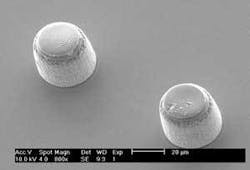
The typical copper post is used in flip chips and similar configurations. The post itself is between 80 and 100 microns tall and around 40 microns wide. On the top of the post is a small dab of solder to provide better bonding with the bond pad on the face of the chip. The body of the post is usually, but not always, encased in epoxy, polyimide, or another underfill material.
Copper-post technology advances
The copper post provides several advantages over tin-lead and lead-free solder bumps. First, because the diameter of the post is not dependent on its height, the copper post is relatively tall and narrow. A solder bump becomes spherical after the molten phase in reflow because of surface tension in the liquid phase, and is essentially a rather fat squashed sphere. The slimmer dimensions of the copper post mean that a much larger number of interconnects can be placed in a given area.
Next, the dimensions of the copper post permit it to be slightly flexible, and therefore capable of handling coefficient of thermal expansion (CTE) differences between the chip and the substrate. A much shorter solder bump might be cracked by the same CTE stresses. The more brittle lead-free solders are probably at greater risk than conventional tin-lead solders.
The copper is more efficient at dissipating heat from the chip than solder bumps would be. The greater height of the copper posts makes it easier to underfill the chip. Shrinking solder bump size and shrinking pitch have left some conventional flip chips with hard-to-underfill offsets of around 35 microns.
Finally, the superior bonding of copper to the substrate, as compared to solder, reduces the likelihood of disbonds.
The assumption is that copper posts will permit the use of higher-performance chips having a far greater numbers of I/Os and having a great deal of heat that must be dissipated. The copper itself improves the efficiency of the thermal path. Although there is little hard evidence to date, it seems very likely that copper post technology will also provide superior long-term reliability.
There are no known uses of copper posts yet in military or aerospace applications, but that day is not far off. Dr. Leonard Schaper, director of the High Density Electronics Center (HIDEC) at the University of Arkansas, is planning to use copper posts in the three-dimensional chip stacking that his team is developing.
“We are part of an AFRL (Air Force Research Lab) program that is looking at the use of 3-D chip stacking in some air force/military systems, particularly things like T-R (transmit-receive) radar modules,” Schaper notes. “And there the need is to handle some high-power gallium arsenide devices in the same stack as silicon devices-and to get power out.
“This is perfect for the copper-post technology, because as the copper post gets rid of some CTE problems, and if you’ve got gallium arsenide and silicon stacked up together and they’re bonded, then you’re right into CTE problems. If they’re separated by copper posts, you can build in some compliance, and that’s the direction we’re going.”
3-D electronics
Schaper’s research will be useful for systems such as phased-array radar operating at very high frequency with densely spaced antenna elements. Performance depends on very high speed signal processing. It is applications such as this that have motivated several recent bit of research into what is called three-dimensional electronics-meaning that the dimensions of a subassembly or system shrink not only in the x and y dimensions (think of printed-circuit boards becoming smaller), but also in the z dimension (think of a stack of thinned chips joined by copper posts).
Although one of the benefits of 3-D electronics is increased miniaturization, the real objective is to reduce wire length. “When I was at Bell Labs we demonstrated that the real driver for cost in electronic systems is the length of wire,” Schaper explains. “And if you can minimize the length of wire in a system, you’re going to minimize the cost. So if I take a system that is now spread out all over a circuit board, and I condense it into a 3-D stack, I’ve reduced the wire length dramatically. So not only do I reduce the latency or the delay, but I think also in the long run, once these are mature processes-I’m not talking about the first experimental ones, but as a mature process-once I have far less wire in my system, I might have far less cost.”
Schaper’s project involves creating a bonded stack that includes gallium arsenide (for high-speed signal reception) and silicon (for signal processing) chips. In conventional packaging terms, a “stack” is an epoxy-encapsulated packaging containing silicon chips that are typically wire-bonded too each other-such a stack is dimensionally compact, but wire-bonding means that there are lots of long wires that slow down processing.
Schaper’s stack bonds the chips to each other using copper posts in place of wires because the copper posts are much faster, and because the copper posts will accommodate the very different CTEs of gallium arsenide and silicon. If the two dissimilar chips were simply bonded to each other, they would be susceptible to bending and cracking.
“You create the wafer first,” he explains. “You put the connection points on the top and bottom, then you dice it, and take parts from maybe several different wafers, and then you assemble them vertically as a chip stack, as a multilayer wedding cake.”
The completed stack might have five to six chips. Schaper prefers to use copper-tin to bond the chips. “Copper-tin is a wonderful eutectic. Once it forms, its melting point is about 200°C higher than its formation point. So if I’ve got two chips and I want to join them together, I do it with copper-tin. Then the next chip that I want to put on top of that, the bonding on the first two doesn’t melt again-unlike solder, which would completely melt again.”
Some researchers have investigated stacking whole wafers rather than stacking individual die, in part because if wafers could be stacked and bonded, 3-D electronics could easily achieve high volume and low cost. But there are two hard-to-surmount problems: it is fiendishly difficult to align the wafers precisely, and the presence of bad chips in random location on multiple wafers means that the yield will be very low.
Through-chip vias
The chip-to-chip connections between the chips in Schaper’s stack are the copper posts, which depend on vias that are etched through the chips and then plated with copper. “The underlying technology is the ability to make through-silicon vias, and a lot of that is copper plating technology. And that same copper plating technology is then used to form the posts, and with a different plating solution to form the tin caps on the posts.
“We’re not seeing much problem in how to put this thing together,” he adds. “In fact, we’ve just been designing a test vehicle for a four-layer stack that’s one centimeter square.”
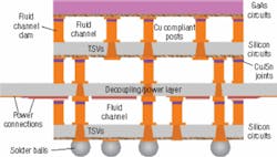
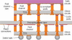
One of the difficulties posed by a tightly bonded stack of chips is the dissipation of heat-a problem that only becomes worse as chip performance escalates. What Schaper has developed can be described as a sequence of hollow copper posts that form a circulation path through which a fluid is pumped. While most of the copper posts serve as electrical interconnects, a few of them are part of the cooling system.
“We also use the same copper post technology to form a fluid channel between each two die,” he explains. “We’ve got space for circulating cooling fluid between every layer of our multi-layer stack. This is the real power of the copper post technology: it allows you to have the compliance for one thing, so I can have gallium arsenide and silicon in the same stack, and it also gives you a way to get the heat out by using a circulating fluid in that channel.
“We’re looking at posts that are 30 microns in diameter and 100 microns high, and that little fluid channel that you create, 100 microns high, we should easily be able to get 100 watts per chip out of the thing. And probably more-that’s the first conservative estimate.”
Schaper anticipates that by Fall 2006 his team will have assembled a stack through which they can circulate the cooling fluid and measure the temperature at each layer of the stack. Assembly is fairly simple and can be done by a standard flip-chip bonder. The assembled stack will contain gallium arsenide and silicon chips, will have very dense interconnects using copper posts, and will be thermally stable.
Advanced signal applications
Although the application of interest is a radar application, Schaper says the advantages of 3-D chip stacking can be used in any advanced signal-processing operation. “It doesn’t matter how you acquire the data, but you really want to work on that data in a way that preserves the spatial relationship among the data points.”
Conventional 2-D data processing-of visual images, sound, IR, radar-doesn’t preserve the spatial relationships, which makes cross-correlations among adjacent pixels impossible, Schaper says.
“But if I can process data in three-dimensional silicon,” he says, “I can come in to the base layer with all of my data on a per-pixel basis coming in on the bottom, and then I can do my processing pipeline vertically and still keep each individual bit of data adjacent to the piece I’m working on. So the spatial relationships are preserved. And I can do those cross-correlations a whole lot faster.”
Aside from advanced signal processing, will 3-D electronics employing through-chip vias and copper posts impact general computing? Schaper thinks it will, because it will make it possible to bring processing functions and memory functions much closer together-another case of removing long wires. “Instead of a 64-bit data bus coming off of a packaged devices and going through the board to a bunch of memory modules, I can have extremely dense z-axis connections up to the memory.
General-computing applications, though, are probably some years in the future. The more immediate applications will center on the need for more powerful radar systems.


