Nanotechnology: the revolution has begun
Nanotechnology, heavily researched and funded across the globe, promises to revolutionize many applications in space flight and communications. The advanced miniaturization concepts will proliferate across many industries in addition to defense and aerospace.
In his novel, "Prey," Michael Crichton scares his readers with thoughts of small nanomachines developing artificial intelligence and attacking humans in swarms like an attack of killer bees or locusts in the desert.
However the reality and promise of nanotechnology is more hopeful than fearful.
Developments in nanotechnology will enable faster computing, biosensors that can detect anthrax, improved medical treatments, ultrasmall sensors, power sources, improving every facet of life from simple household appliances to improved navigation and propulsions systems for future space transportation.
Nanotechnology represents the ability to systematically organize and manipulate matter at nanoscale. Payoff is anticipated within the next 10 to 15 years, say scientists at the NASA Ames Research Center in Moffett Field, Calif. They define it as "the creation of functional materials, devices, and systems through control of matter on the nanometer-length scale (1 to 100 nanometers), and exploitation of novel phenomena and properties (physical, chemical, biological, mechanical, electrical, and so on) at that length scale."
"One nanometer is approximately 10,000 times smaller than an average human hair," says Dr. Mya Meyyappan, director of the Center for Nanotechnology at NASA Ames. Another comparison is the hydrogen atom itself, which is 0.04 nanometers and proteins are approximately 1 to 20 nanometers, Meyyappan adds.
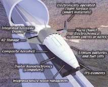
The revolutionary miniaturization in electronics and computing will enable reconfigurable, autonomous, "thinking" spacecraft, NASA officials claim. "Nanotechnology presents a whole new spectrum of opportunities to build device components and systems for entirely new, bold space architectures such as networks of ultrasmall probes on planetary surfaces —microrovers that drive, hop, fly, and burrow — and collections of microspacecraft making a variety of measurements," Meyyappan states, along with Harry Partridge and T.R. Govindan in a white paper, Nano and BioTechnology Research at NASA Ames.
"Nanotechnology — in its various forms such as nanoelectronics, nanoelectromechanical systems, ultrasmall and highly sensitive sensors, multifunctional materials, biologically in spired materials, systems, and architectures, and possibly many others scientists have not yet thought of — is expected to play a strong and critical role in future space transportation and exploration. Also, the intersection of nano, bio, and information technologies provides rich possibilities for exploring useful concepts and breakthroughs," Meyyappan says.
"I would say the revolution will really be felt in about 15 years," Meyyappan says. Right now it has little market share and is mostly still in laboratories and will make incremental progress.
Technology breakthroughs need to be "shaked and baked in a lab for 10 to 12 years before people have the ability to make large quantities with large scalable manufacturing," Meyyappan says. "It is an enabling technology because its impact will be pervasive in so many areas."
Nanotechnology touches many markets
In their 2003 report, Nanotechnology Marketplace Analysis, analysts at Frost & Sullivan in Washington say that nanotechnology will have a major influence on many market sectors.
Sectors that are currently looking closely at nanotech possibilities include the pharmaceuticals and biotechnology industries, as well as computer-hardware companies. In essence, however, almost any form of manufacturing could eventually make use of the processes that are being developed, they said.
According to Frost & Sullivan analysts, developing nanotech-based markets include:
- electronics and computing — which includes the creation of denser hard drives, smaller and faster chips, and better optical equipment;
- chemicals and materials — plastic nanocomposites may be among the first commercial applications in this sector, while battery-scale energy storage as in nanostructured fuel cells is another area;
- defense and security — which includes a range of applications in sensors, surveillance, detection, and communications;
- medical and healthcare — which includes gene and protein array–based diagnostics based on DNA, viruses, and proteins, as well as medical prosthetics made of nanomaterials;
- fabrication and instrumentation — which includes the development of tools (nanometrology) and techniques (new kinds of lithography) that facilitate the development, manipulation, and detection of submicroscopic objects; and
- consumer — which includes apparels made of novel fibers and fabrics with multifunctionality, food, cosmetics, and even sporting goods."
According to a conservative estimate, about 250 companies across the globe are involved in nanotechnology while the majority — more than 100 — is in the single largest field of chemicals and materials (nanomaterials), Frost & Sullivan researchers said in the report. "The overall competitive landscape is significantly fragmented with small, startup companies comprising at least 60 to 80 percent of the market.
"Based on National Science Foundation (NSF) estimates, it is expected that by 2015 nanotechnology markets will represent $440 billion per year in chemicals and materials, $70 billion per year in defense and aerospace, $300 billion per year in electronics and computing, and $180 billion per year in medicine and healthcare, and the total market for nanotech-enabled products and services might reach $1 trillion," according to the report. "The NanoBusiness Alliance, giving more specific forecasts, expects that materials, tools, and manufacturing will drive nanotech industry revenues close to $25 billion by 2006. However, the speed of innovation and the growth of nanotechnologies will fluctuate widely from industry to industry, with some, such as nanomaterials, commercializing significantly faster than others."
Some breakthroughs have already quietly appeared. For example, engineers at General Motors in Detroit are "experimenting with passive nanomaterials for making new footboards and other auto parts," Frost & Sullivan analysts note.
"It is expected that in the next five to seven years, we will see the development of biosensors for detecting DNA, protein, lipids, and anthrax. Given the security perceptions there is likely to be an enormous demand for biosensors," Frost & Sullivan officials say.
In the electronics and semiconductor market, "new microprocessors and other computer chips are technically already close to being called nanotechnology products because the average size of their internal circuits are already reaching 90 nanometers. Faster than current chips, these chips are largely made of the same materials and function in a similar manner," the report says.
The precursors to nanotechnology in electronics are microelectromechanical systems (MEMS) and the market for these devices is growing about 20 to 30 percent each year, says Michel Merluzeau, principal analyst, Aerospace & Defense Group at Frost & Sullivan in Washington. Key players in this area are Crossbow in San Diego and Athena in Warrenton, Va.
IBM has a nanotechnology application for data storage targeted for release in 2005. Company engineers have developed a postage stamp–size memory device that can store approximately 25 million textbooks, Frost & Sullivan analysts say.
Carbon nanotubes
One the most exciting areas of nanotechnolgy is the work being done on carbon nanotubes.
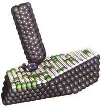
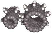
"A carbon nanotube (CNT) is a tubular form of carbon," Meyyappan says. Most people are familiar with carbon in its powder form, compacted in a pencil, or as a natural synthetic — a diamond, he explains.
It is configurationally equivalent to two-dimensional graphene sheets rolled into a tube. It is grown now by several techniques in the laboratory, NASA officials say.
CNTs were discovered only within the last 15 years or so, Meyyappan says. "The diameter can be as small as one nanometer and its length can be anywhere from 10,000 to a million or even billion times larger than the diameter."
"In another ten to 15 years, carbon nanotubes will probably be incorporated into microprocessors, gradually replacing copper wires," Frost & Sullivan analysts state in their report. "Not only would this make computer chips faster and more energy-efficient, they would likely be cheaper to produce. With current chip manufacturing methods, each transistor has to be precisely laid down through lithography, a time-consuming process that costs billions of dollars. By contrast, carbon circuits will form themselves, with the process being controlled through the laws of physics and chemistry."
Carbon nanotube–based molecular electronics will enable high processor speeds without the heat concerns of today's processors. Silicon-based chips today run almost to a terabit but they are so hot "you could boil an egg or make coffee on them," Meyyappan says.
That is why carbon nanotubes are so versatile — they not only have the thermal conductivity properties conducive to high-performance electronics, they are also useful for the material that forms a spacecraft, he says.
"It is one-sixth the density of steel yet 100 times stronger than steel," Meyyappan says.
"In the early days of nanotechnology research, CNTs were primarily grown by laser ablation and carbon-arc techniques by various research groups across the world," Meyyappan says. "Both approaches produce single-wall CNT in small quantities scraped off the cooler walls of the tube. In the last few years, chemical vapor deposition (CVD) has emerged as an alternative approach. CVD, a workhorse in silicon microelectronics, is ideally suited to grow nanotubes on patterned substrates if one is interested in investigating nanoelectronic devices or sensors. NASA Ames operates two CVD reactors to grow nanotubes on substrates.
"The unique properties of CNT make it an attractive candidate for several nanotechnology innovations," Meyyappan says. "The possibility of nanoscale etching using CNT tips has been investigated through molecular dynamic simulations. Selective atomic-scale etching as well as indentation of silicon surfaces by CNT tips have been shown to be possible. Parallelization of an array of tips has the potential to revolutionize future-generation lithography.
"In addition to CNT, the Ames group has also been investigating boron nitride nanotubes, for electronics and structural applications," Meyyappan says.
NIST and nanosized thin films
Researchers at the Commerce Department's National Institute of Standards and Technology (NIST) are working on determining whether thin films — some no thicker than a single molecule — are strong enough for a growing number of nanotechnology applications.
Carbon nanotube (CNT) is a new form of carbon, configurationally equivalent to two-dimensional graphene sheet rolled into a tube. It is grown by several techniques in the laboratory and is just a few nanometers in diameter and several microns long.
CNT can be metallic or semiconducting and offers possibilities to create future nanoelectronics devices, circuits, and computers.
CNT exhibits extraordinary mechanical properties: the Young's modulus is more than 1 Tera Pascal and is stiff as diamond. The estimated tensile strength is 200 Giga Pascal. These properties are ideal for reinforced composites and nanoelctromechanical systems (NEMS).
Useful for evaluating all types and combinations of materials, the new method measures and analyzes the strength and stiffness of a thin-film sample in about two seconds, as compared with several minutes for indentation and other conventional approaches, NIST officials say. In addition, the NIST-developed technique accommodates high-throughput testing, so that hundreds or even a few thousand systematically varying samples can be tested in rapid succession.
Accelerated testing could spur progress in a large variety of existing and emerging technology areas that rely on thin-film advances for improved performance or enhanced protection. Examples include prospective nanotechnology devices semiconductors, solar cells, fuel cells, coatings, and magnetic storage devices.
Called SIEBIMM (for strain-induced elastic buckling instability for mechanical measurements), the new method builds on the science of buckling, which for most of its 400 years has been concerned with crumbling buildings or crumpling of the Earth's crust, NIST officials say.
The method entails mounting a postage stamp–sized assortment of incrementally varying thin films on a strip of silicone rubber about the size of a Band-Aid. The combination of sample array and soft substrate are placed on a custom-built stage that can be stretched or compressed, NIST officials explain.
Subjected to a gradually increasing force that stretches or squeezes, a sample becomes unstable and buckles, wrinkling like a piece of corrugated cardboard. Situated beneath the stage, a laser beams through the sample and a camera captures the light scattered at this critical point of instability.
From the resulting diffraction pattern, the buckling wavelength, or distance between the peaks of adjacent wrinkles, is determined. Through a series of mathematical calculations, the buckling wavelength can be related directly to the elastic modulus of the sample, which corresponds to the strength of the material, NIST officials say.
NIST and IBM collaborators report on how they used the "measurement platform" to assess the strength of polymer and ceramic films ranging from a few nanometers to a micrometer in thickness. One pilot-tested film was a ceramic material dotted with nanometer-scale pores. Such nanoporous films are being developed to insulate devices and layers on future-generation integrated circuits, NIST officials say.
Using the desk-top testing platform, "smaller than a box of tissues," the team evaluated a battery of low-k films that varied in porosity, from samples with no pores to samples in which pores made up half the volume. After comparing the results with those obtained with the nanoindentation method, the team concluded that the NIST-developed approach "provides an inexpensive, fast, and highly effective technique" for evaluating new varieties of low-k materials.
"We expect that this technique will find application in addressing a variety of questions ranging from fundamental materials science to applied discovery in the field of films and coatings," they state in their report.
Christopher Stafford, a NIST polymer scientist, says other applications include evaluations of new photoresist masks that will be used to print chips with the smaller-wavelength ultraviolet light sources that the semiconductor industry is now implementing. It also should be useful for assessing the mechanical properties of nanotechnology devices made with still-experimental methods, such as nano-imprint lithography in which nanometer-scale features are stamped into a substrate.
"This simple technique can provide invaluable information concerning the mechanics of nanostructured materials and ultrathin polymer films," Stafford says.
The SIEBIMM method was developed at the NIST Combinatorial Methods Center (www.nist.gov/.combi), which develops rapid, high-throughput technologies to accelerate the discovery and application of new materials.
Global competition
Analysts at Frost & Sullivan in Washington in their 2003 report, Nanotechnology Marketplace Analysis, state that global nanotechnology research and development "investment reported by government organizations has increased approximately five times in the last five years, between 1997 and 2002, and currently stands in the vicinity of $4 billion. No less than 30 nations have initiated national activities in this field."
According to the report, industry players are confident that nanotechnology will bring competitive advantages. "Worldwide annual industrial production in the nanotech sectors is estimated to exceed $1 trillion in 10 to 15 years from now, which would require about 2 million nanotechnology workers."
However, different governments have different ways of doing things.
"Although the United States has initiated a multidisciplinary strategy for the development of science and engineering fundamentals through the National Nanotechnology Initiative, Europe and Japan, on the other hand, have broad programs backed by government, combining academic- and industry-led R&D, and their current plans look ahead by four to five years," Frost & Sullivan analysts state in their report.
The Europeans are clearly in the lead when it comes to nanotechnolgy investment, Frost & Sullivan analysts report. "A new study from the European NanoBusiness Association (ENA) notes that Europe is outspending the United States on nanotechnology funding by a factor of two. The ENA study is the first analysis of European Union spending on nanotech."
The study was released in 2002 and did not include the fact that European spending received a boost when the European Commission gave $685.4 million for nanotech research, officials at Frost & Sullivan say.
The U.S. National Nanotechnology Initiative has requested $710.2 million for fiscal year 2003.
Funding really became a government focus under the Clinton administration, and the Bush administration has given it even greater attention — recognizing the tough competition from the rest of the world, says Dr. Mya Meyyappan, director of the Center for Nanotechnology at NASA Ames Research Center in Moffett Field, Calif.
The U.S. is accustomed to having the technological advantage over the rest of the world, but with nanotechnology the playing field is fairly even and breakthroughs could come from any part of the globe, Meyyappan adds.
There is also a lot of interest in nanotechnology in Asian countries, particularly Japan, China, Taiwan, Singapore, and South Korea, Frost & Sullivan analysts say. "For example, the Japanese government, which regards nanotechnology important for rejuvenating the stagnant Japanese economy, is expected to spend around $1 billion in 2003. In fact, many Japanese companies are earmarking big money. Over 10 Japanese companies already have nanotechnology research centers/initiatives. The Hitachi Institute estimates that businesses related to nanotech in Japan could be worth several billions of dollars within the next decade."
During the next five years, the "Chinese central government will allocate approximately $240 million while local governments will allocate $240 million to $360 million for nanotech research, the report states. As for Taiwan, the government's National Nanotechnology Initiative will spend about $680 million over the next six years. Taiwan's Industrial Technology Research Institute also spent about $300 million to establish the Center for Applied Nanotechnology. The Singapore government itself has taken a proactive role in nanotech and is acquiring promising companies around the world, such as Surromed — a biotech-nanotech startup in the U.S., the Frost &Sullivan report states.
The other major player, South Korea, "invested close to $150 million into nanotech in 2002, almost double that invested over the previous year. Notably the government has earmarked $10 million a year for the next decade for nanotech memory chips. This is similar to Australia where the government has identified photonics as a key growth area and an area for federal investment," the report states.
"Overall, in this economic environment, government budgets are tightening and private investment is overtaking," the Frost &Sullivan report states. "While spending under the U.S. government's National Nanotechnology Initiative (NNI) has seen double-digit growth over the past couple of years, and has risen to about $700 million (in 2003), most of this money went to university research and government labs. On the other hand, venture capital in the private sector is estimated to reach $1.2 billion by 2003, a sharp rise from the $100 million in 1999.
"Until nanotech delivers the next 'big' thing (some experts expect a nanotech boom in the coming two to four years), it will continue to compete for funding with biotech/medicine and other technologies," Frost & Sullivan analysts say.
For nanotechnology, tool and equipment producers are an important focus of early investments, analysts say. "Since these nanometrological aids such as atomic-force and scanning-tunneling microscopes are enabling technologies (used to manipulate things on the nanoscale), which help in the development of newer nanoprocessors, nanoarrays, and biochips."
ENSCO engineers design microprobes with MEMS to monitor Earth's atmosphere
Engineers at ENSCO in Melbourne, Fla., are designing microprobes to study atmospheric conditions for NASA. The probes, called Global Environmental MEMS Sensors (GEMS), are so small they can be suspended in the atmosphere and carried by wind currents for long periods of time.
ENSCO has recently launched a new business area that focuses on the integration of microelectromechanical systems (MEMS) and nanotechnologies for the design and development of airborne wireless probes/probes networks with GEMS as the initial thrust. In addition to weather/climate analysis and prediction, potential applications include intelligence gathering, homeland defense (threat monitoring and assessment), ground-based monitoring (land or water), and planetary exploration/space environment monitoring.
ENSCO does not manufacture its own MEMS geochronology, but outsources and licenses it from outside fabrication facilities, says Mark Adams, director of nano/bio engineering.
Company engineers have just completed Phase I of the work granted by the NASA Institute for Advanced Concepts (NIAC) and have announced the award of a Phase II continuation, as well as plans for future applications of the technology.
Once suspended in the atmosphere, the GEMS probes would measure meteorological parameters including temperature, pressure, moisture, and wind speed then relay that data back to Earth via a wireless communication protocol yet to be developed, ENSCO officials say. Resulting improvements in forecast accuracy would translate directly into cost benefits for the weather-sensitive space launch and aviation industries, and mitigate the risk factors associated with life-threatening weather phenomena such as hurricanes, floods, tornadoes, and severe storms, they claim.
GEMS can be deployed from an airplane or, if conditions are right, released from the ground and have them float up to the desired altitude, says Adams.
The group will use observing-system simulation experiments to explore issues relating to the deployment and dispersion of probes as well as the impact of probe data on regional meteorological forecasts.
Technological advancements in MEMS and nanotechnology inspired ENSCO engineers to propose GEMS. The system features "micron-scale" airborne probes that can take measurements over all regions of the Earth with unprecedented spatial and temporal resolution, ENSCO officials claim.
Potential applications include: homeland security (threat monitoring and damage assessment), monitoring of space assets for potential and man-made threats in space, ground-based monitoring on land and water, defense intelligence gathering, environmental monitoring, urban warfare, weather and climate analysis and prediction, battlesphere monitoring and surveillance, and exploration of the solar system and beyond.
Based on specific applications, the probes will be designed as small as 50 to 100 microns in one or more dimensions and "lightweight enough to pose virtually no danger upon contact with persons or property," company officials say. The size, mass, aspect ratio, component geometry, buoyancy control, and aerodynamic design will determine how long probes remain airborne.
A key factor is to determine how much nanotechnology to embed in the probe without exceeding power and weight requirements to get the device to float in the air, Adams says.
Each probe will be self-contained with a power source consisting of batteries, fuel cells and/or solar power to provide sensing, data processing/computation, location/navigation, and communication functions. Materials science will play a key role to limit probe mass and potentially make them biodegradable or at least bio-inert, thereby minimizing risks to the environment when the probes settle out of the atmosphere, ENSCO officials claim. They say they expect GEMS to be mass-produced at very low per-unit cost.
The biggest challenge is to get them to communicate with one another so they can function together and extrapolate a picture of the atmosphere and its conditions from different angles, says John Manobianco, GEMS program manager at ENSCO.
The probes will communicate with other probes, remote receiving platforms, and data collectors using radio-frequency (RF) and/or optical-frequency transmissions to form a wireless, mobile network. As part of a wireless network, the probes do not require recovery to collect data, and therefore will be disposable and low cost. "Ten to 20 years from now they should cost anywhere from $1 to 10 cents," Manobianco says. The first initial device is approximately two years away, he adds.


