Company receives second U.S. patent for radiation-hardened zinc oxide thin-film transistors for space uses
INDEPENDENCE, Mo. – Intellectual Property Developers (IPD) LLC in Independence, Mo., has patented the company's zinc oxide thin-film transistors technology for radiation-hardened applications in space.
IPD has received approval for a second patent from the U.S. Patent and Trademark Office in Alexandria, Va. for the ZnO Radiation-Hardened Thin-Film Transistors Technology, says IPD President Vincent Salva.
ZnO Rad-Hard Thin-Film Transistors Technology is for use in electronic components used in satellites, crewed space stations, deep-space exploration, and nuclear power plants, and related applications where there is an atmosphere for radiation exposure damage to electrical components.
IPD developed ZnO rad-hard thin-film transistor technology together with Auburn University in Auburn, Ala.
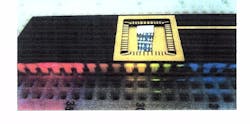
A thin-film transistor is made up of an annealed layer comprising crystalline zinc oxide, with a passivation layer adjacent to the thin-film transistor. The passivation layer has a thickness and material composition such that when a dose of radiation from a radiation source irradiates the thin-film transistor, a portion of the dose that includes an approximate maximum concentration of the dose is located within the annealed layer.
The annealed layer has a thickness and threshold displacement energies after it has been annealed such that a difference between a transfer characteristic value of the thin-film transistor before and after the dose is less than a first threshold; and a difference between a transistor output characteristic value of the thin-film before and after the dose is less than a second threshold. The thresholds are based on a desired performance of the thin-film transistor.
The ZnO technology is radiation-hardened upon irradiation of gamma-ray radiation, and is intended for radiation hard electronics applications in space, nuclear power facilities, high-altitude aviation, and other radiation environments.
ZnO technology offers reduced volume, mass, and power consumption that can operate in extreme temperature ranges.
ZnO technology compares favorably to silicon carbide (SiC), gallium nitride. ZnO technology is relatively inexpensive to synthesize device quality materials compared to GaN or SiC, IPD officials say.
The company has completed a two-year research project, which shows that ZnO transistors are working well under exposure in difficult radiation situations. A patent for ZnO technology has been approved by the U.S. Patent and Trademark Office in Alexandria, Va.
For more information contact Vincent Salva, president of IPD LLC, by email at [email protected], or by phone at 816-254-6670.
About the Author
John Keller
Editor-in-Chief
John Keller is the Editor-in-Chief, Military & Aerospace Electronics Magazine--provides extensive coverage and analysis of enabling electronics and optoelectronic technologies in military, space and commercial aviation applications. John has been a member of the Military & Aerospace Electronics staff since 1989 and chief editor since 1995.
Voice Your Opinion!
To join the conversation, and become an exclusive member of Military Aerospace, create an account today!

Leaders relevant to this article: