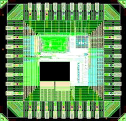
Georgia Tech eyes VLSI compute-in-memory accelerator for artificial intelligence (AI) image recognition
ARLINGTON, Va. – U.S. military researchers needed compute-in-memory accelerator technology based on very large-scale integration (VLSI) fabrication for applications such as artificial intelligence (AI)-based image recognition. They found their solution from Georgia Tech Research Corp. in Atlanta.
Officials of the U.S. Defense Advanced Research Projects Agency (DARPA) in Arlington, Va., announced a $9.1 million contract to Georgia Tech on Monday for the Optimum Processing Technology Inside Memory Arrays (OPTIMA) project.
Georgia Tech will try to demonstrate area- and power-efficient high-performance multiply accumulate macros with signal-processing circuits and architectures.
Accelerators based on von Neumann architecture have limited computational power efficiency and long execution latency, while compute-in-memory architectures with multiply accumulate macros can address these limitations. Still, these implementations have been hindered by the large physical size of memory devices and the high power consumption of peripheral circuitry.
Related: DARPA approaches industry for new battlefield network algorithms and network protocols
The computational power efficiency, expressed in tera-operations per second per Watt of von Neumann general-purpose processors is limited by data movement between memory and computation -- particularly for matrix-vector-multiplication intensive applications.
Tensor processing units and graphics processing units offer alternative architectures exploiting parallelism, but their power efficiency and throughput still are limited by the digital computation and data transfer.
Computer scientists recently have explored compute-in-memory architectures to keep data movement and computing energy at a minimum by employing memory devices such as multiply compute elements. Multiply accumulate macros carry out the parallel matrix summing calculations of the multiply compute element outputs.
Compute-in-memory architectures with arrays of multiply accumulate macros for parallel processing can enhance performance for applications such as AI-based image recognition, yet compute-in-memory implementations have been limited by the large size of multiply compute element memory devices and by the multiply accumulate macro power-hungry peripheral circuitry that is optimized for conventional circuit architectures.
To enable compute-in-memory accelerators with 300 tera-operations per second per Watt computational power efficiency and 20 tera-operations per second per square millimeter of computational area density, Georgia Tech experts will develop a small power-efficient multiply compute element; and a small, scalable, and power-efficient multiply accumulate macro architecture.
Innovations in multiply compute element and multiply accumulate macro are necessary to overcome the technical challenges. Georgia Tech will aim at developing single-transistor-size VLSI multiply compute elements by capitalizing on the transistor transconductance gain for compact in-memory multiply compute elements with speeds faster than 1-nanosecond read access. Such devices could be transistors with built-in memory functions; 3D multiply compute elements with single transistor size.
Georgia Tech also will try to develop signal processing circuits and architectures like mixed domain and stochastic compute processing, and co-optimizing with the OPTIMA multiply compute elements to keep size and power consumption to a minimum.
Related: Optical computing -the next revolution
OPTIMA is a 4.5-year three-phase program that will involve several contractors, so additional contracts are expected. In the project's first phase, Georgia Tech seeks to develop a low-energy single-transistor-size multiply compute element with 1 femtojoule per bit energy to data ratio, five-nanosecond read speed, six F2 nominal size, and 1,010 read endurance.
The second phase will try to improve the multiply compute elements to 0.5 femtojoules per bit energy to data ratio, one-nanosecond read speed, 3 F2 nominal size, and 1,011 read endurance. Phase 3 will develop a compute-in-memory accelerator with 100 tera-operations per second throughput and 300 tera-operations per second per Watt energy efficiency.
For more information contact Georgia Tech Research Corp. online at https://gtrc.gatech.edu, or DARPA at www.darpa.mil.
About the Author
John Keller
Editor-in-Chief
John Keller is the Editor-in-Chief, Military & Aerospace Electronics Magazine--provides extensive coverage and analysis of enabling electronics and optoelectronic technologies in military, space and commercial aviation applications. John has been a member of the Military & Aerospace Electronics staff since 1989 and chief editor since 1995.
Voice Your Opinion!
To join the conversation, and become an exclusive member of Military Aerospace, create an account today!

Leaders relevant to this article:
