Researchers to boost manufacturing for three-dimensional heterogeneously integrated (3DHI) microelectronics
ARLINGTON, Va. – U.S. military researchers are asking industry to develop manufacturing capability for three-dimensional heterogeneously integrated (3DHI) microelectronics in attempts to spur the next major wave of microelectronics innovation.
Officials of the U.S. Defense Advanced Research Projects Agency (DARPA) in Arlington, Va., have issued a solicitation (DARPA-PA-24-03) for the Next-Generation Microelectronics Manufacturing (NGMM) Phase 1 and Phase 2 project.
The DARPA Microsystems Technology Office seeks to establish a domestic capability for research, development, and production of 3DHI microelectronics, with the goal of sustaining U.S. leadership and innovation in microelectronics manufacturing.
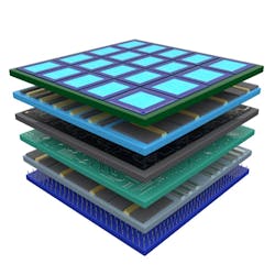
The next major wave of microelectronics innovation is likely to come from integrating heterogeneous materials, devices, and circuits through advanced packaging to produce a tightly coupled system that extends into the third dimension with performance that exceeds what is available from today’s monolithic approach.
The NGMM program will advance the state-of-the-art in 3DHI microelectronics by forming a domestic open-access prototyping and pilot line center accessible to users in academia, government, and industry.
The first and second phases of the NGMM program will take five years. The first phase will focus on establishing baseline fabrication processes, a three-dimensional assembly design kit (3D-ADK), and electronic design automation (EDA) and simulation software tailored to 3DHI.
The second phase will create hardware prototypes, automate processes, and develop emulation and digital twin capabilities. The goal is to create a non-federal self-sustaining 3DHI manufacturing center that is accessible to users in academia, government, and industry to help design high-performance 3DHI microsystems quickly and at reasonable cost.
Industry leaders today use 3D integration of modestly dissimilar silicon digital technologies for a narrow range of commercial products, from stacked dynamic random-access memory (DRAM) to complementary metal-oxide-semiconductor (CMOS) imagers to high-performance computing.
Today’s mature integration techniques, even those often referred to as 3DHI, focus primarily on low-power leading-edge CMOS, legacy CMOS, and silicon-based memory. Still, the opportunity to improve defense systems relies on expanding the types of microelectronics that can be integrated and assembled. Advancing digital integration requires increasing interconnect densities well beyond today’s state-of-the-art.
The U.S. today has no open-access center with capacity for sustained 3DHI research and development. With very few exceptions, U.S. companies engaged in 3DHI research rely on offshore facilities.
An open-access domestic center for 3DHI research could promote an expansive wave of innovation, promote shared learning, and ensure that start-ups, academia, and defense companies could engage in 3DHI research for low-volume products. DARPA researchers say they expect to select one contractor for the $420 million first phase, and for the $420 million second phase.
Companies interested should submit full proposals no later than 5 March 2024 to the DARPA BAA website at https://baa.darpa.mil. Email questions or concerns to [email protected]. More information is online at https://sam.gov/opp/aaf4e3022be14cdf98425a3beae20327/view.
