MEMS industry shakes down into 'Big 4'
By John Rhea
WILMINGTON, Mass. — A wave of mergers and acquisitions in the microelectromechanical systems (MEMS) industry is cresting this year and is creating a "Big Four" of competitors to exploit this technology for optical switching and other leading-edge communications applications.
All four have roots in the telecommunications industry, and two are based in Canada: Lucent Technologies in Murray Hill, N.J., which was the original Bell Telephone Laboratories research arm of AT&T; Nortel Corp. in Brampton, Ontario, which acquired two U.S. firms this year; JDS Uniphase in Nepean, Ontario, which acquired another U.S. firm plus a Motorola wafer fabrication facility; and Corning Inc. of Corning, N.Y., a major fiber optics supplier.
The MEMS industry traditionally has been fragmented. Some companies work on a broad range of low-volume, exotic technologies under military sponsorship. The chief promoter of military MEMS technology is the Defense Advanced Research Projects Agency (DARPA) in Arlington, Va.
Other companies, meanwhile, are fulfilling their own needs through captive facilities, such as Hewlett Packard of Palo Alto, Calif., for its line of inkjet printers, and IBM Corp. in Armonk N.Y., for personal computers. Merchant market suppliers such as Dallas-based Texas Instruments serve the high-volume needs of the automotive industry.
As MEMS technology evolves, the companies beginning to dominate are stressing telecommunications (hence the quest for the all-optical switch) and biomedical and other microminiature instrumentation applications. These products may be available to military users later as commercial off-the-shelf (COTS) commodities.
Nortel last year bought Xros (rhymes with the Tiros weather satellite) of Sunnyvale, Calif., which will serve as its design shop, and CoreTek in Wilmington, Mass., which will handle device fabrication.
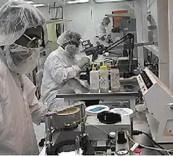
Corning leaders, meanwhile, bought one-third of privately held InteliSense Corp., also in Wilmington, Mass., last year and bought the other two-thirds last June. InteliSense is a one-stop shopping center spanning design and modeling, development engineering, and fabrication in its own 50,000-square-foot cleanroom facility. InteliSense will serve as an in-house supplier to Corning and a merchant market producer.
JDS Uniphase officials in March completed their acquisition of Cronos Integrated Microsystems (named for the Greek god of time) in Research Triangle Park, N.C. This is a MEMS design and prototype wafer fab facility that was spun off a year earlier from the Microelectronics Center of North Carolina (MCNC), also based in Research Triangle Park. In June JDS bought a 177,000-square-foot wafer fab in the same industrial park from Motorola to provide Cronos with a volume production facility.
The maturing MEMS industry is focusing on three primary manufacturing techniques: bulk micromachining, surface micromachining, and high-aspect ratio micromachining (HARM). The difference between surface micromachining and HARM involves thickness: surface micromachining is from 2 to 6 microns thick, and HARM is at least 200 microns thick.
A German-pioneered technology known as LIGA uses X-ray and optical processes. LIGA is the German acronym for lithographie (lithography) galvanoformung (electroplating) and abformung (molding).
To get prototype parts into the hands of potential users and to jump-start the MEMS industry, Cronos has been participating in DARPA's original Multi-User MEMS Processes (MUMPs) program, in which designers can buy part of a wafer to fabricate their devices.
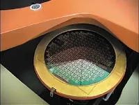
This involves contracting for die measuring about a centimeter square on a wafer, which several companies share. Then the companies receive small quantities of piece parts for evaluation, explains Karen Markus, vice president of technology at Cronos.
The MUMPs process reduces cost and risk, she says, and helps the companies meet the critical need to expedite time-to-market.
The industry consolidation and standardization of process technologies in MEMS mirror long-standing trends in the microelectronics industry. Breakthrough products create markets, and well-prepared companies exploit them.
A study prepared last year by System Planning Corp. in Arlington, Va., sheds light on this process. "MEMS, unlike mainstream electronics, requires a large market for the specific end product, not just for the generic technology," the report notes.
"A useful analogy might be to consider application specific integrated circuits," the study goes on. "The market for an ASIC is clearly much smaller than that for a more general-purpose [integrated circuit] like a Pentium chip," the study concludes. "In MEMS today, everything is like an ASIC."
Experts at InteliSense, partially owned by Cronos, work on all facets of MEMS design.


