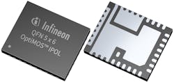
Integrated point of load (IPOL) buck regulators for data storage and distributed power offered by Infineon
MUNICH – Infineon Technologies AG in Munich is introducing a family of OptiMOS 5 integrated point of load (IPOL) buck regulators for next-generation server, data storage, telecommunications, data communications, and distributed-power applications.
These buck regulators offer VR14-compliant SVID standard and I²C/PMBus digital interfaces for Intel and AMD server CPUs and network application-specific integrated circuits (ASICs) and field-programmable gate arrays (FPGAs).
A buck step-down switch-mode voltage regulator has a lower output voltage than its input voltage. It is a DC-to-DC power converter that steps down voltage while stepping up current from its input to its output. It is housed in a 5-by-6-cubic-millimeter PQFN package.
The OptiMOS IPOL single-voltage synchronous buck regulator TDA38640 supports an output current as strong as 40 amps. The device comes with Intel SVID and I²C/PMBus digital interfaces and can be used for Intel VR12, VR12.5, VR13, VR14, IMPVP8 designs, and DDR memory without significant changes to the bill of materials (BOM).
The TDA38740 and TDA38725 digital IPOL buck regulators support output currents as strong as 40 and 25 amps respectively, and come with a PMBus interface.
All three devices use Infineon’s proprietary fast constant on time (COT) pulse width modulation (PWM) engine to deliver transient performance while simplifying the design development.
Related: VPT introduces radiation hardened point of load converters
The onboard PWM controller and OptiMOS FETs with integrated bootstrap diode make these devices a small footprint solution with efficient power delivery. They also operate in a broad input and output voltage range while offering programmable switching frequencies from 400 kHz to 2 MHz.
A multiple time programming (MTP) memory allows customization during design and high-volume manufacturing, significantly reducing design cycles and time-to-market. They also offer a digitally programmable load line that can be set via configuration registers without external components, resulting in a simplified BOM.
The device configuration can be easily defined using Infineon’s XDP Designer GUI and is stored in the on-chip memory. For more information contact Infineon online at www.infineon.com.

