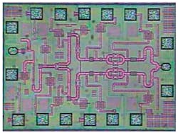
HRL Laboratories to refine millimeter-wave gallium nitride (GaN) integrated circuit technologies for RF uses
ARLINGTON, Va. – U.S. military researchers are asking integrated circuit experts at HRL Laboratories LLC in Malibu, Calif., to refine RF and microwave circuitry for aerospace and defense applications.
Officials of the U.S. Defense Advanced Research Projects Agency (DARPA) in Arlington, Va., announced an $8.4 million contract modification to HRL on Tuesday for phase-two of the Millimeter Wave GaN Maturation (MGM) program.
This initiative seeks to improve RF and microwave semiconductor technologies to improve device yield, reduce process cycle time, and demonstrate key millimeter wave power amplifiers and mixed-signal circuits in multi-project wafer runs (MPWs).
MGM is making strategic yield and reproducibility improvements that capitalize on standard evaluation circuits (SEC), process control monitors (PCM), and short-loop fabrication to identify process step improvements.
In the project's first phase, HRL experts began maturing their RF and millimeter-wave gallium nitride (GaN) semiconductor technologies that they demonstrated during the DARPA Nitride Electronics NeXt-Generation Technology (NEXT) program a decade ago.
The goal of the project's second phase is to reduce the fabrication cycle time, improve the RF yield and reliability, improve device models and the process design kit, and increase the manufacturing readiness level (MRL) of GaN millimeter-wave circuitry.
HRL experts will mature this GaN technology by making targeted process step improvements. They will use process control monitors; make several multi-project wafer (MPW) runs; and improve monolithic microwave integrated circuit (MMIC) design capabilities at the company's their Malibu, Calif., facility.
As a performer on the DARPA NEXT program HRL developed state-of-the-art GaN transistors with scaled gate lengths of 40 nanometers and demonstrated ft/fmax of 200/400 GHz.
The NEXT program sought to develop a revolutionary nitride transistor technology with an extremely high-speed and high-voltage swing of Johnson Figure of Merit (JFoM) larger than 5 THz in large-scale circuit integrations of at least 1,000 transistors.
The project sought to develop fabrication processes that are manufacturable, high-yield, high-uniformity, and highly reliable. The program focused on demonstrating the ability to combine these devices into a small logic circuit of about 10 transistors, and then work up to about 1,000 transistors.
During the MGM project's first phase, HRL updated design kits to support several computer-aided design (CAD) tools, supported multi-project waver runs, and reduced overall fabrication cycle time to support U.S. military users.
This contract modification brings the total value of the MGM contract to HRL to $18.8 million. HRL experts will do the work in Malibu, Calif., and should be finished by September 2022.
For more information contact HRL Laboratories online at www.hrl.com, or DARPA at www.darpa.mil.
About the Author
John Keller
Editor-in-Chief
John Keller is the Editor-in-Chief, Military & Aerospace Electronics Magazine--provides extensive coverage and analysis of enabling electronics and optoelectronic technologies in military, space and commercial aviation applications. John has been a member of the Military & Aerospace Electronics staff since 1989 and chief editor since 1995.
Voice Your Opinion!
To join the conversation, and become an exclusive member of Military Aerospace, create an account today!

Leaders relevant to this article:
